This thread has been locked.

If you have a related question, please click the "Ask a related question" button in the top right corner. The newly created question will be automatically linked to this question.

TPS7B82-Q1: Design requirements and Example Schematic Design For my requirements - TPS7B82-Q1

Part Number: TPS7B82-Q1

Hi team,

The datasheet for the TPS7B82-Q1 IC indicates fixed outputs of 2.5V, 3.3V, and 5V. However, the datasheet lacks configuration details and formulas.

Could you provide guidance on how to configure this IC?

For my design, the input voltage is 9V.

If the required output is 5V means what is  the design requirement.

Similarly, if 3.3V is needed means what is the requirement.

In buck converters, we configure the Output voltages, by configuring the Feedback resistor to the FB pin.

But here there is no pin like this.
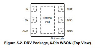
So please provide the Design details in deatil.

Providing a schematic would be very helpful and appreciated.

Thank you.

  • Hello,

    Since the outputs you have specified are fixed output voltage options, there is no configuration necessary. The part should automatically regulate to the fixed voltage option that you purchased. Example: If you purchased the 5V output option device, then the device should automatically regulate to the 5V fixed voltage option. 

    We do have adjustable LDOs, not with the TPS7B82 device, that use a FB pin and a resistor network. An adjustable LDO allows for output voltage options that may not necessarily be fixed. 

    Best Regards,

    Hannah