This thread has been locked.

If you have a related question, please click the "Ask a related question" button in the top right corner. The newly created question will be automatically linked to this question.

UCC27712: high and low mos be turned on at the same time

Part Number: UCC27712

hello,

I use two ucc27712 to build a full H-Bridge.I tested the circuit today and i found some question.

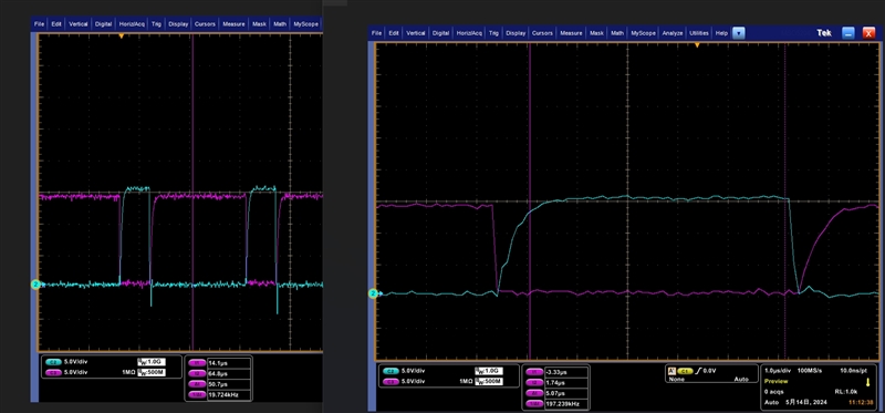
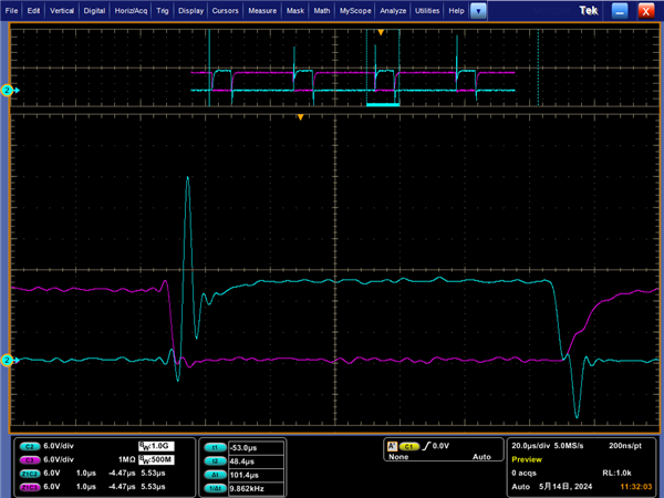
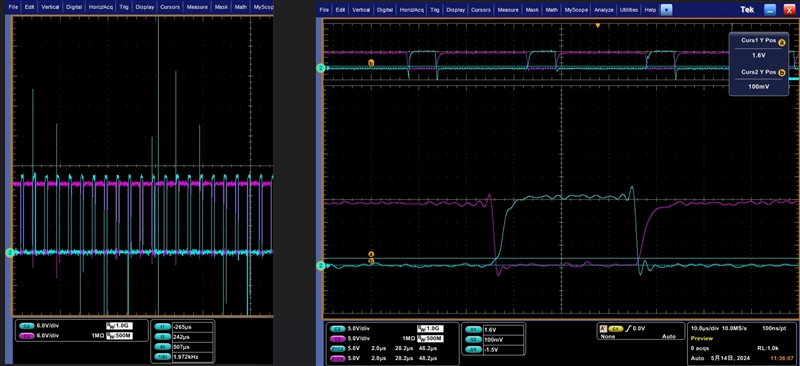
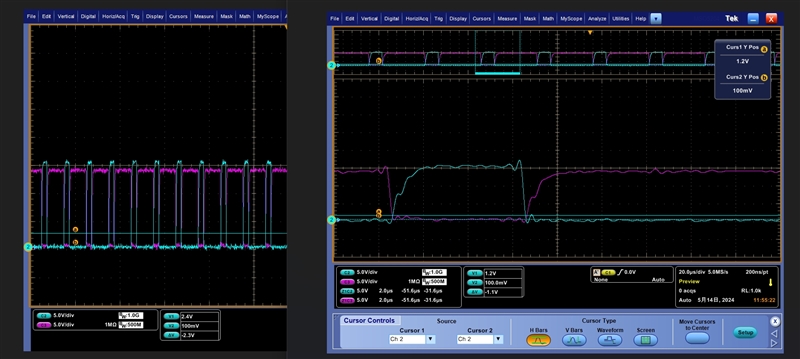
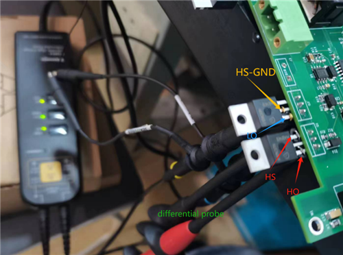
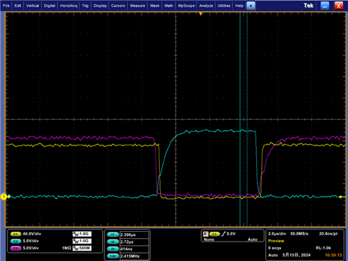
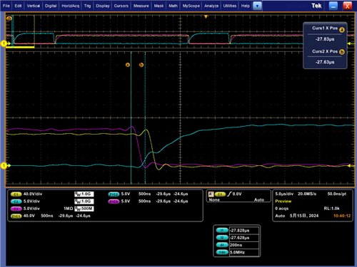
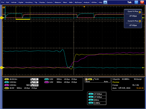
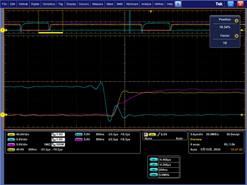
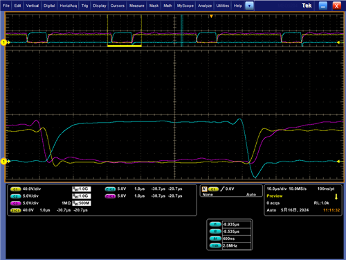
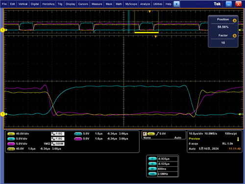
i first found the mosfet became hot when i diaconnected the load,and then i tested the output of the ucc27712,HO and LO waveform are as follow

i cannot understand the step during the falling of the output,and I think it is this reason that causes the upper and lower MOS to be turned on at the same time, causing them to heat up.

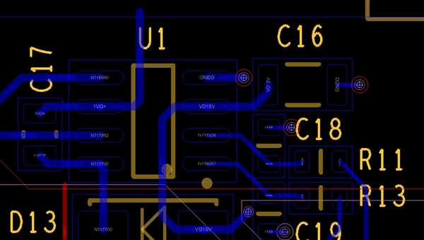
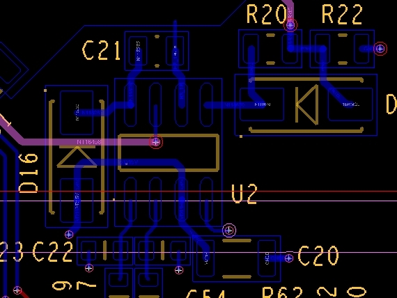
my schematic is as follow.part number of the mos is IPP410N30

i also tested the delay of the 74HC4049 and the value is about 8ns.

please help me

  • Hey,

    Thank you for reaching out to TI regarding your questions related to the UCC27712.

    I have a few questions to better help me understand your situation.

    1. Are you measuring HO with respect to HS via a differential probe? The high-side is level shifted to be referenced to HS and so the Vgs of the high-side FET is HO-HS. If you do not have a differential probe, you can measure HS-VSS and HO-VSS and use a math channel on the scope to determine HO-HS.

    2. Are C16 and C20 placed close to the gate driver? They need to be in order to source current for the high load transients. Also, these should be X7R ceramic capacitors and the value of 47uF is much larger than expected. With a 0.1uF bootstrap capacitor, we recommend using a bypass capacitor of 10 times larger than the bootstrap capacitor that is X7R for C16 and C20. 

    3. What is the deadtime between your HI and LI input signals?

    Let me know if you have any questions.

    Thank you,

    William Moore

  • Hello,

    thanks for your reply.

    1 i tried some conditions ,i use i differential probe to measure HO-HS(purple line),a normal probe to measure LO-VSS(blue line)

    a IPP410 NMOS,40kHz PWM,C16&C20=47uF,VD96=30V,the waveform is as follow

    b vd96v=96V

    there are too many spur,but i donot know why

    c i changed c16&c20 value to 1uF

    d i found a board earlier than zhe IPP410 and the mos part number is IRFB4127(IPP410 is delivered later than IRFB4127),the only difference is the nmos

    4127+1uf(C16&C20)+40kHz+96V,waveform is follow

    during test,i found the mos became hot in 1 monute and the temperature rise was over 40 degree.the mos irfb4127 is lower,but they also became warm.

    2 my layout is as follows

    3 i only use one pwm signal as the high pwm and i use a inverting gate to generate the low pwm.

    my question:

    1 i cannot understand why the two mos cause the difference of the waveform

    2  i want to know what should i do to resolve this problem of the spur and the problem of hot mos

    thanks very much

  • Hey,

    Can you take a waveform capture that includes HO-HS, LO-VSS and HS-VSS?

    What is the status of the HS switch node during this testing? Is it left floating?

    It appears that HS is still high during the LO rising edge and causing the body diode to conduct until LO goes high and can pull HS low. This would create a lot of switching losses which could result in the heat you are seeing.

    For the overshoot on the rising edge of LO, it appears that you are seeing that with the IPP410N30N. This could be due to the lower gate charge and the larger difference in the Miller charge.

    Where and how are your measurements being taken? Are they taking at the pins of the gate driver with a tip and barrel probe?

    Let me know if you have any questions.

    Thank you,

    William Moore

  • hello,

    my HS is floating because I don't have the load that our customer is asking for.

    i repeated the test and took these pictures:the yellow line is HS-VSS,purple line is HO-HS,blue line is LO-VSS:test board is the one use irfb4127

    when i test this with another board,i found a different waveform of the LO signal,the signal rises after the falling edge

    1 I think you are right,the HS is still hign during the lo rising edge. how can i resolve thie issue? 

    2 how can i reduce the LO rising after falling edge?if i replace the ipp410n30 with another NMOS whill work?(IRFB4127 Vds-break is 200V and it isnot match my need)

    thank you

  • Hey,

    1. The reason HS is still high during the LO rising edge is due to the switch node (HS) being floating, so there is nothing to pull it down to ground whereas if there was an output stage connected to it in a no load condition, it would be able to pull HS to ground.

    2. To adjust dV/dt of rising/falling edges, this is done by changing gate resistances. But this additional rising edge on LO that you are seeing after the falling edge can be due to the Miller charge of the other half bridge when a high dV/dt rising edge is seen causing this false pulse. A lower gate charge (Qg) FET will have a faster rising edge for turn on.

    Have you tried this in a no load condition with the output stage connected and HS not floating?

    Do you see this issue when there is a load also?

    What you are seeing is likely due to MOSFET parasitics instead of gate driver operation as the gate driver appears to be operating as expected.

    Let me know if there are any questions.

    Thank you,

    William Moore

  • hello,

    i tested the circuit with a smaller load.The actual load is an electromagnet with an inductance of about 800mH, and I use a 100mH inductor in series with a 40R 50W power resistor instead. i use the full bridge to test it.

    the ipp410 circuit waveform is as follow

  • Hey,

    It appears that with the load, the undershoot does not result in a rising edge which is good and this only occurs with the IPP410N30N.

    This MOSFET has lower Qg and therefore will slew faster for the rising and falling edges than the IRFB4127.

    To reduce this undershoot on LO, you can increase gate resistance of the turn-off path which is through the turn off diode. Also, you can add a clamping Schottky diode to help limit this undershoot as well.

    The case of the Miller Charge of the other half-bridge causing this false pulse that I mentioned earlier is still relevant here.

    Let me know if you have any questions.

    Thank you,

    William Moore

  • thank you very much for your help.