This thread has been locked.

If you have a related question, please click the "Ask a related question" button in the top right corner. The newly created question will be automatically linked to this question.

TPSI3050: Designing with TPSI3050

Part Number: TPSI3050
Other Parts Discussed in Thread: TPSI3052, , TPSI3052-Q1

Hello Team,
We are planning to design a circuit using the IC TPSI3050.
Can you please confirm the use of the pin PXFR.
The datasheet says it controls the power transfer to the VDDH pin.
Please correct me if I am wrong.
The maximum duty cycle we can obtain is 93%.
Does this mean the VDRV pin will be low during the 7% time of the 25uS?.
The datasheet says "setting EN pin to a logic low causes VDRV to be driven low.".
So if we supply the EN pin with a 3.3V (100% ON time), will the VDRV also be 100% time ON?.
If the power transfer is for 93% time, how can the VDRV pin can be 100% time ON?.

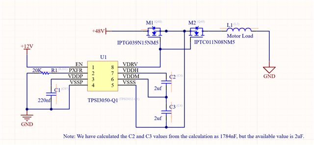
In our application, we need bidirectional current flow. So we are planning to use back to back FET as in the image below.
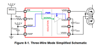

The MOSFET part number is IPTC011N08NM5.
We need 100% ON time for the device.


Looking for your reply

  • Hello Sv,

    Thanks for reaching out to our team on E2E! Don't worry about the power transfer duty cycle, just input the system specs into the calculator tool and check the power transfer tab. The TPSI305x-Q1 transfers power (set by RPXFR) which is stored as charge in CDIVx. Every time the TPSI305x-Q1 drives a MOSFET, it pulls charge from CDIVx, so it is necessary to size CDIVx adequately in order to minimize droop. 

    So if we supply the EN pin with a 3.3V (100% ON time), will the VDRV also be 100% time ON?.

    Yes, setting EN high 100% of the time will also set the driver high 100% of the time. The duty cycle on EN directly corresponds to the duty cycle on VDRV.

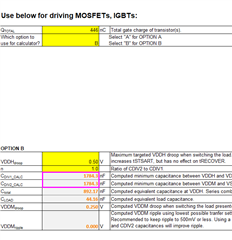
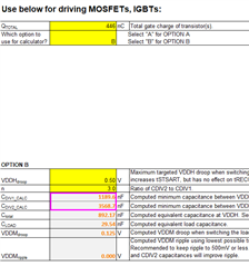
    For your selected back-to-back MOSFETs, I'm seeing that CDIVx should be at least 1.5 µF each. And the various power transfer levels correspond to the different start-up times, recovery times, and maximum possible switching frequencies highlighted in pink below.

    Best regards,
    Tilden Chen


    Solid State Relays | Applications Engineer

  • Hello Team,
    Thank you for your reply.
    If I understood your reply correctly, the bootstrap capacitors (CDIV1 and CDIV2) will transfer the energy to the MOSFET gate during the remaining 6.7% time of the 25uS?.
    Please correct me if I am wrong.

    Also, the datasheet says, the VDRV pin can deliver up to 1.5A of current and can sink 3A of current.
    The power source of the VDRV is from the VDDH pin which is supplied from the VDDP pin.
    Since the device is acting like a boost converter, that is from 5V at the VDDP pin to 10V across the VSSS and VDDH pin, the input current must be very high to get a 1.5A output current. In the datasheet it is only about 40mA.
    Can you please confirm the same?.
    We are planning to provide a 3.3V at the VDDP pin.

    The MOSFET we are planning to use is IPTC011N08NM5.
    Can you please size the value of the CDIV1 and CDIV2 in three wire mode?
    In our application, we have back to back MOSFETs.
    Also, we have TPSI3050 and TPSI3052.
    Which one will be more suitable for our application.

    The MOSFETs are used to switch 48VDC.
    So when the MOSFET is ON, the VSSS pin will be at 48V and the VDDH pin will be at 48+10VDC.
    Is there any problem with this?
    I hope since the secondary side is isolated, we don't have any problem with this.
    Can you please confirm the same?


    What is the maximum current through EN pin when in three wire mode?

  • Hello Sv,

    Thanks for your reply here. 

    If I understood your reply correctly, the bootstrap capacitors (CDIV1 and CDIV2) will transfer the energy to the MOSFET gate during the remaining 6.7% time of the 25uS?.
    Please correct me if I am wrong.

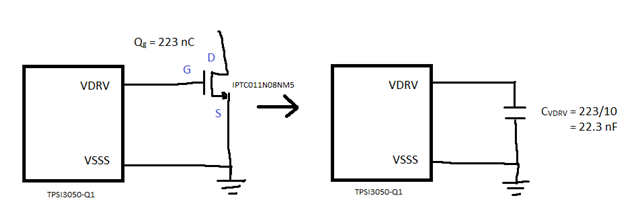
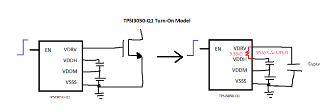
    You can ignore the 25-µs, this is not relevant to the driver switching timing. We can model switching a MOSFET as charging and discharging a capacitor (CVDRV), the value is determined by the total gate charge (Qg) divided by the driver voltage (VDRV). Every time we turn on the MOSFET, this is the same as charging up CVDRV to 10 V. Every time we turn off the MOSFET, we discharge CVDRV

    Also, the datasheet says, the VDRV pin can deliver up to 1.5A of current and can sink 3A of current.
    The power source of the VDRV is from the VDDH pin which is supplied from the VDDP pin.
    Since the device is acting like a boost converter, that is from 5V at the VDDP pin to 10V across the VSSS and VDDH pin, the input current must be very high to get a 1.5A output current. In the datasheet it is only about 40mA.

    When the TPSI305x-Q1 drives VDRV high, it basically connects VDDH to VDRV. When the TPSI305x-Q1 drives VDRV low, it pulls VDRV to VSSS. The  peak source and sink currents (1.5A/3.0A) can approximate what the internal resistance looks like for pullup/pulldown.

    The MOSFET we are planning to use is IPTC011N08NM5.
    Can you please size the value of the CDIV1 and CDIV2 in three wire mode?

    In the calculator tool, I'm taking 2x Qg = 2x 226 nC = 446 nC.

    For TPSI3050-Q1, should probably use CDIV1 = CDIV2 = 2 µF

    For TPSI3052-Q1, should probably use CDIV1 = 1.5 µF, CDIV2 = 4.7 µF

    Also, we have TPSI3050 and TPSI3052.
    Which one will be more suitable for our application.

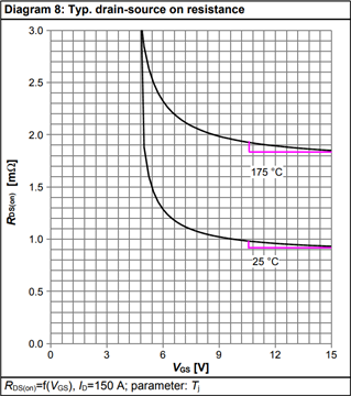
    I think this will depend more on how much MOSFET enhancement you need, which depends on how much power the MOSFET needs to handle. I see less than 0.1-mΩ delta in RDSON between VGS=10-V and VGS=15-V, so I think either TPSI305x-Q1 device would be fine.

    The MOSFETs are used to switch 48VDC.
    So when the MOSFET is ON, the VSSS pin will be at 48V and the VDDH pin will be at 48+10VDC.
    Is there any problem with this?
    I hope since the secondary side is isolated, we don't have any problem with this.
    Can you please confirm the same?

    Can confirm this will be fine.

    What is the maximum current through EN pin when in three wire mode?

    EN under 5-V sees 1-MΩ, so 3.3-V/1-MΩ = 3.3-µA.

    Best regards,
    Tilden Chen


    Solid State Relays | Applications Engineer

  • Hello Tilden,
    Thank you for your detailed response.

    When the TPSI305x-Q1 drives VDRV high, it basically connects VDDH to VDRV. When the TPSI305x-Q1 drives VDRV low, it pulls VDRV to VSSS. The  peak source and sink currents (1.5A/3.0A) can approximate what the internal resistance looks like for pullup/pulldown.

    1). I still have some doubts regarding the 1.5/3A current.
    Does this current is the output current through the VDRV pin to the GATEs of the back back MOSFETs?.
    If so, it has to be supplied from the VDDP pin or the bootstrap circuit.
    Please correct me if I am wrong.
    The output current (to the GATE of the external MOSFET) is directly connected to the turn ON time of the MOSFET.
    If so what is the maximum gate current we are able to obtain in order to get the fast turn ON time of the external MOSFET?

    2). In 2 wire mode with TPSI305x-Q1 device, what will be the current through the EN pin?.
    In 3 wire mode we will have the 10/15V output even if the EN is low. So more power is wasted.
    So we are planning to go with 2 wire mode.

    3). In 2 wire mode, will we able to get 10/15V at VDDH w.r.t VDDS when the EN is powered from an 8V supply.

    4). I am curious to know the same TPSI305x-Q1 IC can sink 2 different current in 2 wire as well as in 3 wire mode.

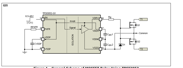
    5). Panasonic recommended GATE resistor for their driver circuit, as shown in the attached snippet. We are planning to use TPSI305x-Q1 (Driver) and IPTC011N08NM5 (MOSFET) for our design. Could you please confirm whether that gate resistor is needed for our design? If it is needed, then how can we calculate the gate resistor for our design?.


    Looking for your reply

  • Hello Sv, 

    Thanks for your reply here. I am out on timebank so future responses may need to wait until May 22nd. Trying to respond now on my phone so apologies if messages are brief.

    1). I still have some doubts regarding the 1.5/3A current.
    Does this current is the output current through the VDRV pin to the GATEs of the back back MOSFETs?.
    If so, it has to be supplied from the VDDP pin or the bootstrap circuit.
    Please correct me if I am wrong.
    The output current (to the GATE of the external MOSFET) is directly connected to the turn ON time of the MOSFET.
    If so what is the maximum gate current we are able to obtain in order to get the fast turn ON time of the external MOSFET?

    Yes, the sourcing current is provided by CDIVx. The maximum gate current would be the 1.5A source but also need to account for resistance in the gate path. I see a 1.6-ohm Rg typical in the datasheet, so I think the maximum current possible here would be directly connected VDRV to MOSFET gate with no external gate resistance, 10-V/(6.6-ohm + 1.6-ohm) = 1.2-A.

    2). In 2 wire mode with TPSI305x-Q1 device, what will be the current through the EN pin?.

    Having trouble sending pictures on my phone, but this depends on PXFR, the datasheet “Electrical Characteristics” section and the calculator tool’s Power Transfer tab show the exact values.

    3). In 2 wire mode, will we able to get 10/15V at VDDH w.r.t VDDS when the EN is powered from an 8V supply.

    Assuming this means w.r.t VSSS, but yes. VDDM, VDDH, VDRV are always w.r.t VSSS.

    4). I am curious to know the same TPSI305x-Q1 IC can sink 2 different current in 2 wire as well as in 3 wire mode

    In both two-wire mode and three-wire mode, RDSON_VDRV is the same. But in two-wire mode, since power transfer happens only when EN is high, CDIVx must charge up each time EN goes high, and VDRV must wait for VDDH to reach VDDH_UV_R (8.3-V for 3050, 13-V for 3052). So for two-wire mode, the peak source current is lower compared to three-wire mode where VDDH charges all the way up to 10-V/15-V. 

    5). Panasonic recommended GATE resistor for their driver circuit, as shown in the attached snippet. We are planning to use TPSI305x-Q1 (Driver) and IPTC011N08NM5 (MOSFET) for our design. Could you please confirm whether that gate resistor is needed for our design? If it is needed, then how can we calculate the gate resistor for our design?.

    I’m not sure, typically gate resistance is to slow down turn-on time. Can you please share the source of this screenshot? Assuming it is from a datasheet.

    Best regards,
    Tilden Chen


    Solid State Relays | Applications Engineer

  • Hello Tilden,
    Thank you for your reply,

    We are planning to use TPSI305x-Q1 (Driver) and IPTC011N08NM5 (MOSFET) for our design and Also,we are going with two wire mode design and below attached schematic snap.kindly check this selected value on this schematic.

    MOSFET Qg = 446nC

    1.what is the minimum & maximum VDRV pin (Iout current)? how can we calculate the Iout current for our design?

    2.Panasonic recommended GATE resistor for their driver circuit, as shown in the attached snippet. We are planning to use TPSI305x-Q1 (Driver) and IPTC011N08NM5 (MOSFET) for our design. Could you please confirm whether that gate resistor is needed for our design? If it is needed, then how can we calculate the gate resistor for our design?.

  • Hello prema,

    Thanks for your rely here. I’m out on timebank so I’ll provide a more in-depth reply when I am back May 22nd. At first glance, those CDIVx values look good. 

    1.what is the minimum & maximum VDRV pin (Iout current)? how can we calculate the Iout current for our design?

    Let me check this when I get back.

    2.Panasonic recommended GATE resistor for their driver circuit, as shown in the attached snippet. We are planning to use TPSI305x-Q1 (Driver) and IPTC011N08NM5 (MOSFET) for our design. Could you please confirm whether that gate resistor is needed for our design? If it is needed, then how can we calculate the gate resistor for our design?.

    We don’t need a gate resistor unless you intentionally want to slow down the MOSFET turn-on time.

    Best regards,
    Tilden Chen


    Solid State Relays | Applications Engineer

  • Hello Tilden,
    Thank you for your reply here,

    I still have some doubts regarding Iout current.

    1.what is the minimum & maximum VDRV pin (Iout current)? how can we calculate the Iout current for our design?

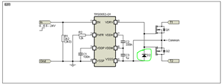
    2. we go through this link https://sound-au.com/project245.htm regarding TPSI305x-Q1 (Driver) they are using diode across VDRV to VSSS.Could you please confirm whether that Diode is needed for our design? and why they are using this diode?

    We need to switch -15V with the back to back MOSFET.

    Is there any problem in switching negative voltage/GND with TPSI3050 using this diode

    kindly refer this attached image or link and let me know.

  • Hi Prema,

    I am another engineer within Tilden's team and would be glad to help!

    To explain the Iout current, there may be confusion because of the name. To help describe the device function:

    In two-wire mode the TPSI3050-Q1 will transfer power slowly across the isolation barrier until Cdiv1 and Cdiv2 are charged.

    Once both caps are sufficiently charged (which is VDDH_UV_R, or around 8.6V), it will use an internal FET to connect the pin 7 to pin 8 (connect Cdiv1, Cdiv2 to VDRV). The impedance of this FET is essentially close to 5-6ohms, hence the maximum gate current out of VDRV will be around 1.5A. As this happens, the capacitors Cdiv1, Cdiv2 will be draining, since current cannot be supplied fast enough from VDDP across isolation to keep it charged. This is fine for driving a MOSFET, since the period of time would be very short (microseconds or milliseconds).

    I hope this helps explain the device function. It can provide high gate current to turn a MOSFET on quickly (it will not get stuck, partially on). In order to do this, it will be storing energy in bootstrap capacitors on the secondary side, and take some period of time to charge them up (in the order of milliseconds, it depends on capacitor size and PXFR setting).

    For 2), the external diode is optional. I do not believe it is necessary since we have a similar diode clamp protection integrated. We do not use it in any of our testing but I understand it is a common method added to many MOSFET gate drive designs. So it may help as an extra level of protection, or may protect an unusual condition we are not considering.

    Thanks,

    Alex

  • Hello Alex,
    Thank you for your reply.
    The application note https://sound-au.com/project245.htm suggest adding a diode D2 for negative voltage protection.

    1). Can you please explain what is this negative voltage condition?.


    , the external diode is optional. I do not believe it is necessary since we have a similar diode clamp protection integrated

    I believe the clamping diode will keep the VDRV pin 2V below the VSSS voltage but not against negative voltage.
    Please correct me if I am wrong.

    2). We are planning to switch negative voltage as well as ground through the back to back MOSFET switches and the MOSFETs are driving using the TPSI3050 device.
    Is there any problem in doing so?.
    3). In 3 wire mode, since we have 10V at the VDDH pin irrespective of the EN pin condition, we are planing to use the 2 wire mode.
    Can you please confirm it will be more power efficient if we go with 2 wire mode?.

    Looking for your reply

  • Hello Sv,

    Thanks for your reply here. 

    I believe the clamping diode will keep the VDRV pin 2V below the VSSS voltage but not against negative voltage.
    Please correct me if I am wrong.

    VDRV should have body diodes to clamp in the negative direction, so D2 is not needed.

    2). We are planning to switch negative voltage as well as ground through the back to back MOSFET switches and the MOSFETs are driving using the TPSI3050 device.
    Is there any problem in doing so?.

    This should be fine since the clamps will prevent the MOSFET from accidentally turning on.

    3). In 3 wire mode, since we have 10V at the VDDH pin irrespective of the EN pin condition, we are planing to use the 2 wire mode.
    Can you please confirm it will be more power efficient if we go with 2 wire mode?.

    2-wire mode is more power efficient since the TPSI305x-Q1 only transfers power when EN goes high. The trade-off is slower turn on time since CDIVx need to charge up from zero. Do you have any switching frequency or turn-on timing requirements?

    Best regards,
    Tilden Chen


    Solid State Relays | Applications Engineer