Hi Team,
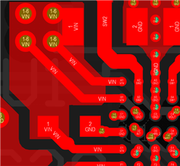
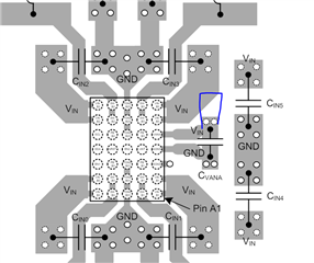
Datasheet tells VANA should be connected to VIN BX pins directly on PCB. However from your layout recommendation it does not directly connected on the top layer. Could i just connect VANA to VIN B3 on top layer?
-A
Hi Team,
Datasheet tells VANA should be connected to VIN BX pins directly on PCB. However from your layout recommendation it does not directly connected on the top layer. Could i just connect VANA to VIN B3 on top layer?
-A