This thread has been locked.

If you have a related question, please click the "Ask a related question" button in the top right corner. The newly created question will be automatically linked to this question.

TPS4811-Q1: Troubleshooting help with attempted implementation

Part Number: TPS4811-Q1

Hello,

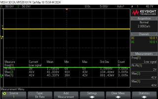
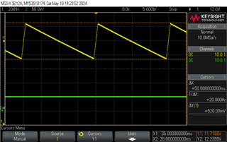
I have attempted to use the TPS48110-Q1 chip for one of my pcb designs for a power supply. However, I am having difficulties getting it to work as expected. The PU/PD pins never go high and so they never turn on the FET that opens to the main power rail. Basically, the system never starts up as the FET never open from the intake. This is because the PU/PD tracks are continuously measured at appx. ground (0V), and never increase. The Charge Pump keeps jumping at around 11.7V, regardless of input voltage, so that part seems to be working fine.

My operating range is 35V to 48V, with 1060W max effect. I have attempted many different ways to troubleshoot, including desoldering certain components.

Results of measurement during troubleshooting:

I have verified that EN/UVLO is within the range 1.2V to 2V (measured at 1.47V with 42V input).
INP pin is also within range 1.6V to 2V (measured at 1.68V).

OVP was measured at 0.974V, which should also be within acceptable range, as it is still below 1.1V which is the OVP_threshold value.


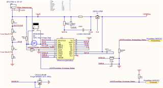
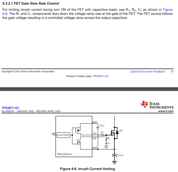
I largely used the datasheet and MATLAB to calculate all the resistors and capacitors, but during my troubleshooting I discovered your Excel-sheet. I have double-checked my calculations with the Excel-sheet, and there are only very minor differences, that should not be the cause preventing system startup.

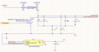
I've been trying to troubleshoot this for several days now, and unfortunately it's already implemented on a PCB, so I've had to desolder components to check. I completely removed the OV input by desoldering R3, and then just adding a 2.4k resistor from R2 to ground to connect the gap after removal. This essentially keeps the voltage divider at the same values, while shorting OV to ground as recommended by the data sheet when not in use - but this had no effect.

I'm scratching my head trying to figure this out, and since I'm essentially out of ideas for troubleshooting now, I decided to reach out here, where I might get more experienced assistance in order to get my system to work. Please let me know if there is anything missing that would help diagnose the issue.

Vin,min = 35V
Vin,nom = 40V

Vin,max=55V

Max effect = 1060W, current depends on operating voltage (30.3A for 35V input, 26.5A for nominal input).
Auto-retry. Transients allowed for 1ms.

Hopefully somebody has some insights.

  • Hi,

    Welcome to E2E!

    Q3 should be a mmbt3904 transistor. Can you connect DIODE pin to gnd and check.

    Do you have any capacitance at the output ? If yes - please remove and try

    Can you share test waveforms of VIN, VOUT, GATE, TMR and input current during startup.

    BR,

    Rakesh

  • Hello Rakesh,

    Thank you for your early reply. There are some capacitors at the output, yes. I will perform your checks and try to record the requested waveforms during startup, then I will get back to you here.

    Regards,
    Bjørge

  • Hello again Rakesh,

    I have made the requested measurements, except for the inrush current as I did not have an appropriate shunt resistor. However, the DC power supply was locked at 6mA. I connected the diode input pins to ground first, as instructed. There was also no capacitance at the output.

    Measurements were done with 43V input. Green probe (2) connected to main input and ground. Yellow probe (1) connected to measurement point and ground.

    Here is the measurement from pin 3, for output voltage:
    Pin 3, Output Voltage

    Measurement from pin 2, for input voltage:
    Pin 2, Input Voltage

    Measurement from pin 3, for gate voltage:
    Pin 3, Output Voltage

    Measurement from CTMR to GND:
    CTMR1

    Second measurement of CTRM to GND using multimeter, since the Peak-to-Peak voltage kept fluctuating from 0V to 3V:
    CTMR2
    With multimeter, it was constantly measured at 226.8mV, as can be seen from the measurement resembling a step function displayed in the multimeter.

    Extra measurement of CBST to SRC:
    CBST

    As for the transistor MMBT2222A replacing the suggested MMBT3904, most values in the datasheet are identical except for a few that i did not expect to be relevant. Shorting it to ground unfortunately did not change anything.

    Please let me know if I should re-do any measurements or change anything else to make it easier to diagnose.

    Regards,
    Bjørge

  • What is the reason to set power supply limit at 6mA? Can you increase to 1A and try.

    Can you check CTMR value. For 1ms you need 68nF not 68pF as seen in your schematic.

    Can you check INP, EN, OVP levels

  • Hello again,

    The current limit was set low to prevent overloading during testing, but I have redone the measurements with increased current (1.5A draw allowed), without much change as it mostly still drew 6-8mA.

    However, shorting the diode FET to ground allowed the main FET to open at around 42V input. Meaning the diode FET was most likely the problem after all, despite having carefully tried to find an equivalent one to the suggestions (pcb factory did not have any in stock of the recommended FET at the time). Thank you for the suggestion.

    So this basically fixed the problem of no conduction/turn-on to main power rail, and the circuit now works (initially) as intended. However, when I connect the following load circuit, the output voltage of Q2 (main power FET) drops from the 42V to a static 5.6V on the output pin, while input voltage pin is still 42V.

    FH1 and FH2 designate holder for a cylinder fuse that completes the connection. The PSU allows up to 3A of current, but only 6-10mA is being drawn even after connecting the load circuit. Since the load circuit has a lot of capacitance, and you asked about this, perhaps this is an issue? Q2 still outputs 42V fine when this circuit is disconnected.

    Thank you for your help so far.

    Regards,
    Bjørge

  • Startup or hot-plugging a capacitive load trigger OCP or SCP event due to inrush current. Please use gate slew-rate control and check.

    Best Regards,

    Rakesh