This thread has been locked.

If you have a related question, please click the "Ask a related question" button in the top right corner. The newly created question will be automatically linked to this question.

ISO5852S: The IC is getting damaged and the VEE and VCC: Possible causes for that

Part Number: ISO5852S

I designed two gate drivers using the IC ISO5852S to be used in a half-bridge LLC resonant converter. One Gate drive is responsible for triggering two switches ( Working in parallel to divide the current on the switches) at the upper part of the leg of the half-bridge, and the other one is responsible for triggering two switches ( again, working in parallel to divide the current on the switches) at the lower part of the leg. A push-pull arrangement is being used after both ICs to boost the current that goes to the IGBTs.The switching frequency used is 80 kHz. the power of the half-bridge converter is 6 kW. 

My team was testing the power circuit and the IC got permanently damaged in the middle of the process. When I checked its terminals, The VEE and the VCC were shortcircuited.

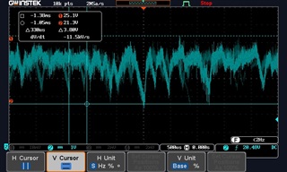
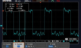
The signal after the ICs (that goes to the Push-pull) was a bit noisy, but nothing really bad. On the IGBTs, it also looked very decent. 

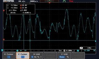
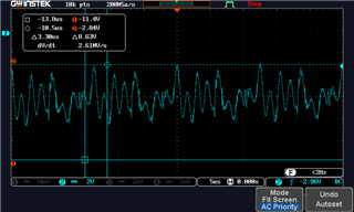
On the other hand, at the input of the IC, the signal at the pin IN+ was very distorted. I tried to filter it with a low pass filter, and I used a Zener diode to limit the maximum and minimum values of the signal, but nothing seemed to work. 

I suspect that the distortion might be related to the source of the input signal. To adapt the setup of a preview prototype, which has the gate drive in a separate board, we are using the output signal of this preview gate drive IC (which is an IR2213) as the input of the IC ISO5852S. The main issue with that is regarding the output of the IR2213. It is an IC designed to be used as a half-bridge driver. Due to that, it has two inputs: the low output is referred to as the ground, and the high output is referred to as a floating point. To turn these two outputs into two inputs for our two ISO5852S ICs, we connected the floating point to the ground, but I always had many doubts about that. We never paid attention to that though, because when we saw the input signals of the ICs ISO5852S without providing voltage (300 V) to the Half-bridge bus (we were analyzing the driver signals, before providing power to the half-bridge circuit), everything was ok, but as soon as the Half-bridge starts operating with its DC bus at its nominal voltage, and at full load, the input signal of the IC ISO5852 gets distorted. It is important to point out that the output supply of the IC is completely isolated from the input supply, due to an isolated DC-DC converter. 

Given the above, I´d like to ask you, what do you think about these input distortions? Does any perturbation on the input could somehow damage the output of the IC and shortcircuit the VEE and VCC?

What are the main causes of this kind of damage in the IC?

Thank you.


  • Hi Vitor,

    Thank you for posting to E2E.

    A noisy input would case the output to have similar glitches if the noise oscillations are long enough for the signals to pass through the input pin de-glitch filters. Even then I wouldn't expect noisy output behavior to cause VCC to VEE shortcircuit specially since you are using a buffer circuit, so there isn't much current going through the gate driver internal output stage.

    A VCC to VEE short-circuit sounds like an overvoltage stress on the VCC or the VEE pin. I have a couple questions to understand the issue better:

    • Could you confirm if the short circuit is between VCC to VEE or is short to different pins?(e.g. VCC to GND2, or VEE to GND2)
    • Is this a repeatable test in your system?
      • If so could you rerun the test by probing the power supplies with a small probing loop to capture noise on these power supplies at the pins of the gate driver?(Try to probe as close to the gate driver pins as possible)

    Best regards,

    Andy Robles

  • Thank you for getting back to me. 

    Regarding your questions:

    1 - I remember that I found both situations. Once, one of our ICs had the pins VCC, VEE, and GND shortcircuited, and at another time, it had only the VCC and VEE shortcircuited. In both cases, could that be related to an issue presented only on the power side of the IC?

    2 - I can run this test. I will send you the results as soon as possible. 

    Best regards,

    Vitor Gontijo

  • Hi Vitor,

    Since it damage associated with the power supply pins of the driver it seems it may be overvoltage/undervoltage transient on these pins. Could you probe the following signals when you try to replicate the damage:

    • Use a small probing loop in order to capture the most accurate representation of the signal going into and out of the gate driver(e.g. MMCX test points or pigtail probing)
      • VDD2-GND2
      • VEE2-GND2
      • VDD2-VEE2
      • OUTH-GND2

    Best regards,

    Andy Robles

  • I can do that.

    I will provide the waveforms as soon as possible.

    If the issue is related to some sort of voltage picks in one of these pins, is a TVS diode enough to solve it?

  • The waveforms requested are despicted below:

    VDD2-GND2

    VEE2-GND2

    VDD2-VEE2

    OUTH-GND2

  • Hi,

    Due to the holiday in the US on 27 May 2024, many of the device experts are currently out of the office. When they return, they will look into this and provide a response. Please expect some delay accordingly.

    Thanks,
    Pratik

  • About the main cause of the failure of the IC, at some point in our tests, we measured the output current, and the waveform looked very unusual, with some current peaks (with a 100ns - 300ns duration) above the IC limits. The equipment worked fine for 20 hours, and then the IC got damaged after that. 
    I'm not 100% sure but at that point, I remember that the GND, the VCC, and the VEE were all shortcircuited. Could these current peaks be the cause of the damage in that preview situation?
    We made several adjustments on the PCB right now, and it doesn't show these issues regarding the output current anymore, but we didn't have tested it yet.

  • Hi Vitor,

    When you say output current do you mean the output current of the gate driver?

    • The gate driver output current is determined by the resistance in the gate loop path. The 2.5A peak source is limited by the internal pull up MOSFETs so I'm not sure which current you are referring to.

    Looking at the supply waveforms you provided there is a lot of noise on the the gate driver supply pins. Proper voltage regulation is important in order to provide the IGBT a stable Gate to source voltage for proper operation.The amount of oscillations and magnitude of the oscillations on these supplies pins are the ones that worry me.

    • Could you provide more details on what were the fixes implemented that seem to remove the issues?

    Best regards,

    Andy Robles