This thread has been locked.

If you have a related question, please click the "Ask a related question" button in the top right corner. The newly created question will be automatically linked to this question.

UCC27714: Power management forum

Part Number: UCC27714

Dear TI Team,
We are facing some issue with UCC27714 driver ( specially at HO & boot caps).

System detail:
Input voltage: 33-34V
Input current :60A
Output voltage: 30V
Output current: 60A( but we are still at 10-15A Only due to this issue)
Switching frequency 230Khz.


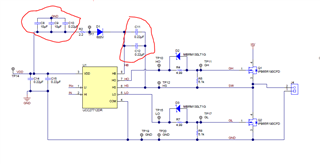
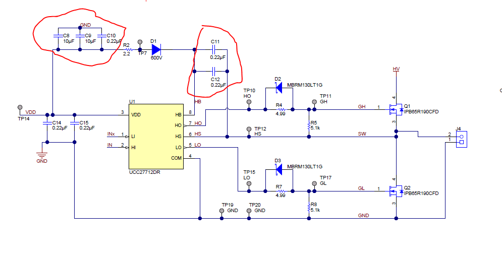
Case 1:
Below is the attached waveform of HI_Pin (Green), HO_Pin (Blue) & HB_Pin ( RED) waveforms.
at 10-15A load it seems working fine, As show in below image.


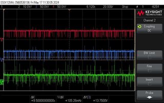
Case2: As we start to increasing load above 15A, then the HO pin waveforms getting corrupted, as shown in below image ( HI_Pin (Green), HO_Pin (Blue) & HB_Pin ( RED) waveforms )
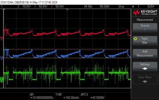


HI ON time ~ 80mSec
HI OFF time ~ 20mSec.


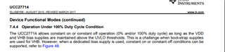
Below is the UCC27714 components details:

1) VDD =12V
2) CVDD=470uF
3) CBOOT = 470nF
4) RBOOT =5R1
5) DBOOT = SS320LWN
6) MOSFET Qg = ~100nC.
7) Rgate = 1R
8) RHI & RLI = 51R
9) CHI & CLI = 220pF

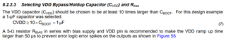
We also tried different CVDD & CBOOT values keeping same DBOOT, RBOOT, VDD etc. But result is the same issue ( Issue still persist)

Case1:
1) CVDD = 1uF
2) CBOOT= 47nF, 100nF & 470nF

Case2:
1) CVDD = 470uF
2) CBOOT= 47nF, 100nF & 470nF

Case3:
1) CVDD = 4.7uF
2) CBOOT= 47nF, 100nF & 470nF


Note: We also monitored the 12V line, it seems constant, there is no change in 12V line nor any fluctuation observed.


  • Hey,

    Thank you for reaching out with your question regarding the UCC27714.

    I have some follow up questions to better understand what your system is and what conditions you are seeing.

    1. It says that you have a 230kHz switching frequency but a HI frequency of 10Hz with HI high for 80ms and HI low for 20ms. Can you please clarify here as your Case 2 scope capture has a time scale of 50ms/div and shows what appears to be more like 10Hz.

    2. For your Case 1 scope capture, I do not see proper operation as you say is shown as this appears to be a very noisy plot. How are you taking your measurements? It is best if you take your measurements as close to the gate driver as possible while utilizing the tip and barrel probe method.

    Let me know your responses to the above and if you have any further questions.

    Thank you,

    William Moore

  • Hey,

    1) Yes, it was 50ms/div & like I said, turn ON time was 80ms and off time is 20ms. But yes switch freq is 230Khz and this on/ off time is not same as switch freq and it seems something different.

    Note: We had measured switch frq it was 230khz.

    2) in case 1 : yes there was a little bit noise but you can consider it is straight high line ( mean  HI always High or may be high till 99% duty and 1% off).

  • Also I would like to know, of HI 100% On for long time, will the HO high? If yes, then how boot cap will charge? Since LO continues off.?

  • Hey,

    You are correct with such high duty cycle and if 100% duty cycle operation is intended, you will need to find a way to bias the high-side. Here is some documentation on how that can be done.

    So the HO and HB waveforms that you are seeing is due to the bootstrap capacitor not being charged up with LO not being on.

    [FAQ] How to bias the high side of a half-bridge gate driver and why

    Let me know if you have any questions.

    Thank you,

    William Moore

  • Hey,

    1) Are you sure this is related to boot strap capacitor not being charged up?

    2) But like as mentioned in data, UCC27714 can support 100% or 0% duty, unless VBH or VDD above UVLO.
    Can you explain on this?

    3) Also could you reconfirm UCC27714 will not support 100% Or 0% duty without any external circuit?

    4) If external circuit is required for 100% or 0% operation, could you suggest alternate device ( pin-pin & package compatible with UCC27714 )  which we can replace 
    it easily. Like you already know our input operating voltage range is below 100V you can also suggest if any driver available in this range, not compulsory required 600V drive for our system.


  • Hey,

    1) This can be checked if you measured HB-HS during this condition and see what the voltage levels are and if it is staying above the UVLO threshold.

    2) Yes, the UCC27714 can support 100% or 0% duty cycle if the voltages on VDD-VSS and HB-HS do not fall below the UVLO thresholds.

    3) Supporting 100% duty cycle requires the external circuitry discussed in the FAQ that I shared above because the bootstrap capacitor cannot source current to drive the high-side gate if it is not recharged during the LO on time.

    4) We do not have a gate driver at this time that can support 100% duty cycle without the external circuitry. This would require a high-side driver, where for these conditions we offer the half-bridge driver with the external circuitry. We do offer a large portfolio of 120V half-bridge gate drivers, but they do not support 100% duty cycle either without the external circuitry.

    Let me know if you have any further questions.

    Thank you,

    William Moore

  • Hey,
    We were checking UCC27714 EVM schematic, but we show parallel CBOOT & CVDD as shown in below image.

    1) Could you please let us know what is the benefit to us topology ?
    2) Is it only to reduce ESR ?
    3) Is recommended design?


  • Hey Shankar,

    The capacitors C8, C9, and C10 are for decoupling and are in parallel with C14 and C15. These are needed for energy storage for biasing VDD. Section 9 Power Supply Recommendations in the datasheet talks more about this.

    Also, Section 8.2.2.3 Selecting VDD Bypass/Holdup Capacitor (CVDD) and Rbias discusses this as well.

    So, these low ESR, ceramic X7R capacitors are recommended design and help ensure that there is enough energy stored to bias the gate drive and not violate UVLO. During 100% duty cycle operation, the charge stored in these would be depleted and violate UVLO. That is why a high side biasing solution is needed as mentioned in the FAQ linked previously.

    Let me know if you have any further questions.

    Thank you,

    William Moore

  • Hey William,
    I think, you did not understand my question.

    1: As per data sheet there should be 3 capacitors on CVDD 100nF, 1uF & 22uF on CVDD  pin, but in EVM why single 22uF was not used and instead of this they used 10uF X 2 ( means, parallel combination). Is it to reduce ESR or any other reason?

    2: This is same for CBOOT capacitors. Means, why 0.22uF X 2 ( means, parallel combination) used and why 470nF single capacitor not used?


  • Hi,

    Due to the holiday in the US on 27 May 2024, many of the device experts are currently out of the office. When they return, they will look into this and provide a response. Please expect some delay accordingly.

    Thanks,
    Pratik

  • Hey Shankar,

    The above schematic that you have included is from the UCC27712EVM which has a power stage but is different from the power stage of that with the UCC27714EVM, so the sizing of capacitances will be different due to different requirements.

    1. I did not design this EVM, but the usage of two 10uF capacitors as opposed to a single 22uF capacitor is because of the ability to select smaller physical sized capacitors which have lower ESR and also better frequency response. Yes the datasheet recommends 3 capacitors for VDD for bypassing, energy storage, and high frequency response.

    2. The selection of a single 470nF capacitor may have worked, but the two 0.22uF capacitors were likely selected due to the same reasons as mentioned in part 1 for CVDD.

    Let me know if you have further questions.

    Thank you,

    William Moore