This thread has been locked.

If you have a related question, please click the "Ask a related question" button in the top right corner. The newly created question will be automatically linked to this question.

TPS546D24A: Compensation settings review

Part Number: TPS546D24A
Other Parts Discussed in Thread: TPS546D24

Hi,

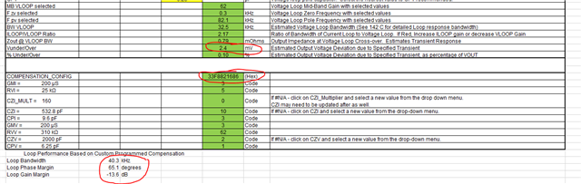
Can you please review my compensation spreadsheet? I'm hoping the loop bandwidth can be improved, and perhaps also phase and gain margin. If I need to adjust the inductor value as well, this is acceptable. I started with a WEBENCH design but I find the compensation calculation to be unreliable (or otherwise not tuned to my particular application).

WBDesign-TPS546D24-12v-2p4v.pdf

12V_MULTI-SLURB01-TPS546x24A_2024-05-17-revA.xlsx

Thanks,

Tom

  • Hi Tom,

    Thanks for filling out the spreadsheet. 

    What you did is correct for choosing Comp Code 20 based on all your other inputs. 

    However, do you really want 14 x 560uF bulk cap and 20 x 100uF ceramic cap? That seems a lot. You would be able to get away with less if you go with higher switching frequency. This will also allow you to set higher loop bandwidth if transient response is critical for your system. 

    Do you have a target phase margin and gain margin? Also, do you have a target steady state output voltage ripple, transient response undershoot/overshoot voltage, etc.? 

    Please let us know all your critical need, so we can help optimize your solution.

    Thank you,
    Tomoya

  • Hi!

    No, I don't want that much Cout...necessarily. While playing with the spreadsheet, I kept adding bulk caps because the "Vunder/Over" was red. We want a very tightly controlled Vout with minimum deviation. As stated in my spreadsheet, I'd like to design in a 5mV ripple for a 3A load step. Note: this is also a test board and will be low quantity, so space and cost are not a big constraint--performance is more important. In other words, although that amount of caps looks a bit silly, if it will help me reach my goals it is perfectly OK to do so.

    Yes, I can raise my Fsw, in fact I was slowly doing that while meeting my target objectives. The WEBench started at 325 kHz and although that's the version I sent out, I expect I should have to go to a higher Fsw, perhaps 550 kHz. But as I raise my Fsw, I'm expecting I will need to change my inductor, and then my design deviates more and more from WEBench.

    Phase margin needs to be above 60 but preferably higher. Gain should be as high as possible without affecting the other metrics. My last design used the same TPS, and with a 5V Vin, 0.3V Vout, the metrics were: BW: 141kHz, Ph.Mar.: 78 degrees, GainMar.:-19dB

    Thanks for your support,

    Tom

  • Hi Tom,

    Thanks for clarifying your use case. Do you know what is the slew rate of the 3A load step? Because the calculator is assuming the di/dt slew rate to be infinite. However, the slew rate is generally finite, so you can expect to see less overshoot/undershoot than what the calculator predicts and may not need those additional output capacitance. 

    Are you using the PMBus at all? If you can use the PMBus for the COMPENSATION_CONFIG configuration, it will give you more options to fine-tune the compensation than what the MSEL1 pinstrap options offers.  Based on my calculation, it looks like you need the VLOOP gain to be higher than 8, which is not available via pinstrap options. 

    First, let us know your load transient slew rate. 

    Thank you,
    Tomoya

  • Hi Tomoya,

    I don't have a defined slew rate. This is a test chip (the load) that does not have well defined parameters. A larger load step is in fact possible (i.e. 20A when the load goes from idle to running a job), but it won't be instantaneous. I think a 3A load step of "near infinite" di/dt is reasonable, however. In the absence of information, I'd like to design conservatively.

    Yes, we will use PMBUS, and from looking at the spreadsheet, I  agree we will likely need a VLOOP gain of >8.

    Thanks,

    Tom

  • Hi Tom,

    Great! If you are using the PMBUS, then what you already had in your original calculator should work fine and gives you the transient performance you need: 

    Vunder/Over is less than 3mV, over 65 degrees of phase margin, and high gain margin. 

    As it's said in the calculator, you will need to configure COMPESATION_CONFIG to 0x33F8821686. 

    If you have any further questions, let us know.

    Thank you,
    Tomoya

  • Hi,

    Can you also review the resistor strap recommendations from the spreadsheet and confirm they are correct?

    For ADRSEL,Rtop=="#N/A", is "Open" the correct setting?

    Thanks for your support,

    Tom

  • Hi Tom,

    Tomoya will help you after he is back on Tuesday. (5/27/24 is TI holiday). Thanks for your patience!

    Thanks,

    Nancy

  • Hi Tom,

    The reason the tool is giving you "#N/A" is because the selected values for the PMBUS ADDRESS and INTERLEAVE was an invalid input.

    If you want the PMBUS ADDRESS = 36d and INTERLEAVE = Auto Detect, then you should leave the ADRSEL pin Open or Floating. 

    Thank you,
    Tomoya