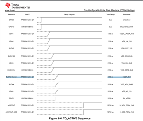
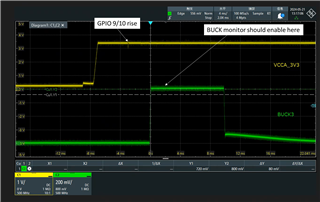
Dear expert,
Customer use TPS65941213 + LP876411B4RQKRQ1.
There is one pcs system cannot power up at -20C. Need your guidance here:
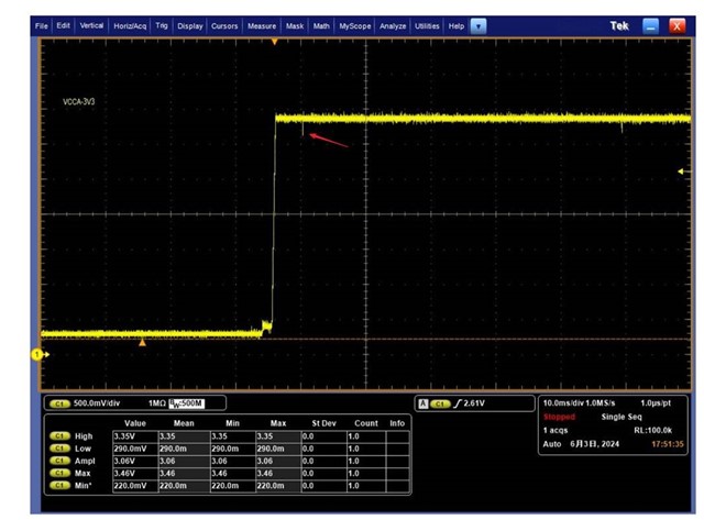
Below is TPS6594 VCCA_3V3 and Buck3 output. After several retry fail, they shut down VCCA_3V3.
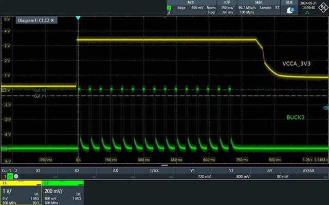
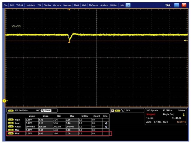
Below is TPS6594 and Buck3 output zoom in.
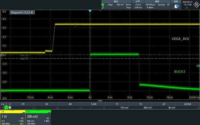
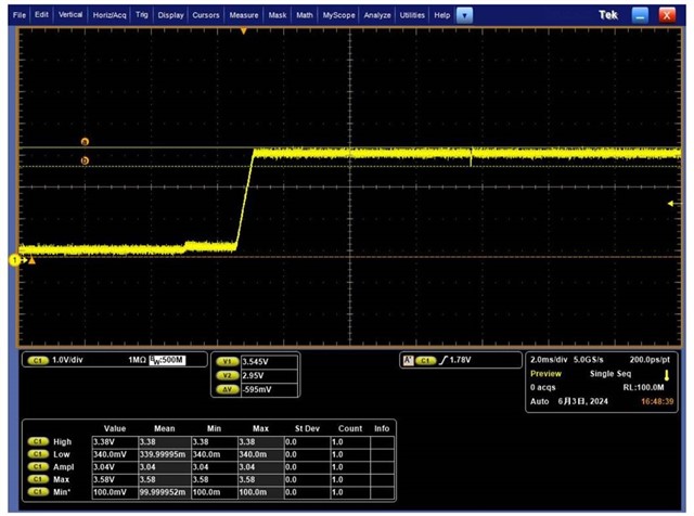
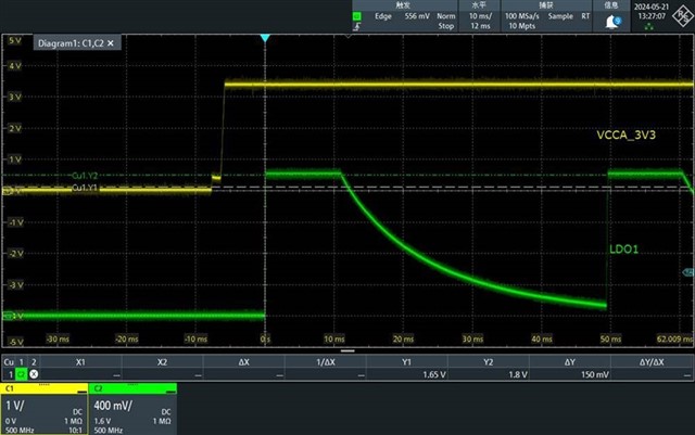
Below is TPS6594 VCCA_3V3 and LDO
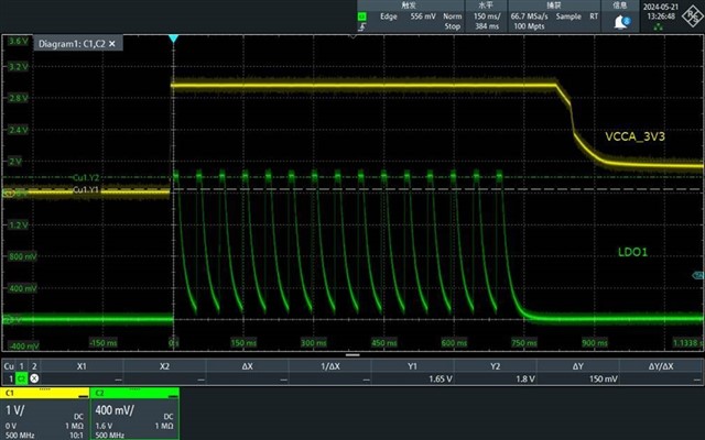
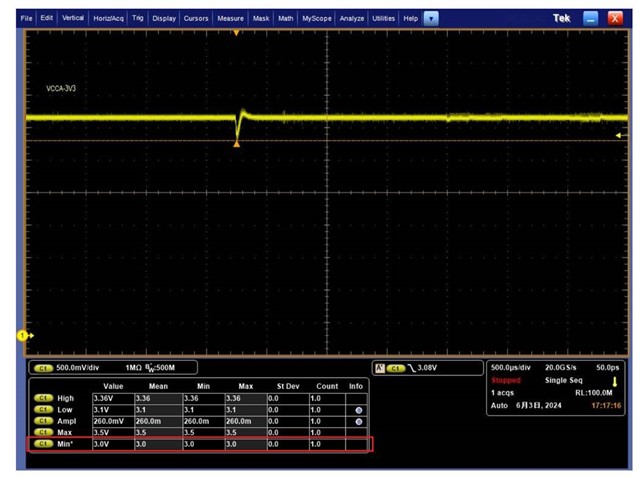
Below is TPS6594 VCCA_3V3 and LDO zoom in:
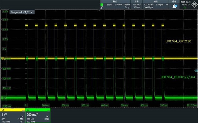
Below is LP8764 Vout and GPIO 10 output
Below is TPS6594 register dump:
|
DEV_REV |
|
0x01 |
|
1 |
0 |
0 |
0 |
0 |
0 |
1 |
0 |
|
|
NVM_CODE_1 |
|
0x02 |
0 |
0 |
0 |
1 |
0 |
0 |
1 |
1 |
||
|
NVM_CODE_2 |
|
0x03 |
0 |
0 |
0 |
0 |
0 |
1 |
0 |
0 |
||
|
BUCK1_CTRL |
|
0x04 |
0 |
0 |
1 |
0 |
0 |
0 |
0 |
0 |
||
|
BUCK1_CONF |
|
0x05 |
0 |
0 |
1 |
0 |
1 |
0 |
1 |
1 |
||
|
BUCK2_CTRL |
|
0x06 |
0 |
0 |
1 |
0 |
0 |
0 |
0 |
0 |
||
|
BUCK2_CONF |
|
0x07 |
0 |
0 |
1 |
0 |
1 |
0 |
1 |
1 |
||
|
BUCK3_CTRL |
|
0x08 |
0 |
0 |
1 |
0 |
0 |
0 |
0 |
0 |
||
|
BUCK3_CONF |
|
0x09 |
0 |
0 |
1 |
0 |
1 |
1 |
0 |
1 |
||
|
BUCK4_CTRL |
|
0x0A |
0 |
0 |
1 |
0 |
0 |
0 |
0 |
0 |
||
|
BUCK4_CONF |
|
0x0B |
0 |
0 |
1 |
0 |
1 |
0 |
1 |
1 |
||
|
BUCK5_CTRL |
|
0x0C |
0 |
0 |
1 |
0 |
0 |
0 |
0 |
0 |
||
|
BUCK5_CONF |
|
0x0D |
0 |
0 |
0 |
1 |
1 |
0 |
1 |
1 |
||
|
BUCK1_VOUT_1 |
|
0x0E |
0 |
0 |
1 |
1 |
0 |
1 |
1 |
1 |
||
|
BUCK1_VOUT_2 |
|
0x0F |
0 |
0 |
1 |
1 |
0 |
1 |
1 |
1 |
||
|
BUCK2_VOUT_1 |
|
0x10 |
0 |
0 |
1 |
1 |
0 |
1 |
1 |
1 |
||
|
BUCK2_VOUT_2 |
|
0x11 |
0 |
0 |
1 |
1 |
0 |
1 |
1 |
1 |
||
|
BUCK3_VOUT_1 |
|
0x12 |
1 |
1 |
1 |
1 |
1 |
1 |
0 |
1 |
||
|
BUCK3_VOUT_2 |
|
0x13 |
1 |
1 |
1 |
1 |
1 |
1 |
0 |
1 |
||
|
BUCK4_VOUT_1 |
|
0x14 |
0 |
1 |
0 |
0 |
0 |
0 |
0 |
1 |
||
|
BUCK4_VOUT_2 |
|
0x15 |
0 |
1 |
0 |
0 |
0 |
0 |
0 |
1 |
||
|
BUCK5_VOUT_1 |
|
0x16 |
1 |
0 |
1 |
1 |
0 |
0 |
1 |
0 |
||
|
BUCK5_VOUT_2 |
|
0x17 |
1 |
0 |
1 |
1 |
0 |
0 |
1 |
0 |
||
|
BUCK1_PG_WINDOW |
|
0x18 |
0 |
0 |
0 |
1 |
1 |
0 |
1 |
1 |
||
|
BUCK2_PG_WINDOW |
|
0x19 |
0 |
0 |
0 |
1 |
1 |
0 |
1 |
1 |
||
|
BUCK3_PG_WINDOW |
|
0x1A |
0 |
0 |
1 |
1 |
1 |
1 |
1 |
1 |
||
|
BUCK4_PG_WINDOW |
|
0x1B |
0 |
0 |
0 |
1 |
1 |
0 |
1 |
1 |
||
|
BUCK5_PG_WINDOW |
|
0x1C |
0 |
0 |
0 |
1 |
1 |
0 |
1 |
1 |
||
|
LDO1_CTRL |
|
0x1D |
0 |
0 |
1 |
0 |
0 |
0 |
0 |
0 |
||
|
LDO2_CTRL |
|
0x1E |
0 |
0 |
1 |
0 |
0 |
0 |
0 |
0 |
||
|
LDO3_CTRL |
|
0x1F |
0 |
0 |
1 |
0 |
0 |
0 |
0 |
0 |
||
|
LDO4_CTRL |
|
0x20 |
0 |
0 |
1 |
0 |
0 |
0 |
0 |
0 |
||
|
LDOINT_CTRL |
|
0x21 |
0 |
0 |
0 |
0 |
0 |
0 |
0 |
0 |
||
|
LDORTC_CTRL |
|
0x22 |
0 |
0 |
0 |
0 |
0 |
0 |
0 |
0 |
||
|
LDO1_VOUT |
|
0x23 |
0 |
0 |
1 |
1 |
1 |
0 |
0 |
0 |
||
|
LDO2_VOUT |
|
0x24 |
0 |
0 |
1 |
1 |
1 |
0 |
0 |
0 |
||
|
LDO3_VOUT |
|
0x25 |
0 |
0 |
0 |
1 |
0 |
0 |
0 |
0 |
||
|
LDO4_VOUT |
|
0x26 |
0 |
0 |
1 |
1 |
1 |
0 |
0 |
0 |
||
|
LDO1_PG_WINDOW |
|
0x27 |
0 |
0 |
0 |
1 |
1 |
0 |
1 |
1 |
||
|
LDO2_PG_WINDOW |
|
0x28 |
0 |
0 |
0 |
1 |
1 |
0 |
1 |
1 |
||
|
LDO3_PG_WINDOW |
|
0x29 |
0 |
0 |
0 |
1 |
1 |
0 |
1 |
1 |
||
|
LDO4_PG_WINDOW |
|
0x2A |
0 |
0 |
0 |
1 |
1 |
0 |
1 |
1 |
||
|
VCCA_VMON_CTRL |
|
0x2B |
0 |
0 |
1 |
0 |
0 |
0 |
0 |
1 |
||
|
VCCA_PG_WINDOW |
|
0x2C |
0 |
0 |
1 |
1 |
1 |
1 |
1 |
1 |
||
|
GPIO1_CONF |
|
0x31 |
0 |
0 |
1 |
0 |
0 |
0 |
0 |
0 |
||
|
GPIO2_CONF |
|
0x32 |
0 |
1 |
0 |
0 |
0 |
0 |
0 |
0 |
||
|
GPIO3_CONF |
|
0x33 |
0 |
1 |
0 |
1 |
1 |
0 |
0 |
0 |
||
|
GPIO4_CONF |
|
0x34 |
1 |
1 |
0 |
0 |
1 |
0 |
0 |
0 |
||
|
GPIO5_CONF |
|
0x35 |
0 |
0 |
1 |
0 |
1 |
0 |
0 |
1 |
||
|
GPIO6_CONF |
|
0x36 |
0 |
0 |
1 |
0 |
1 |
0 |
0 |
0 |
||
|
GPIO7_CONF |
|
0x37 |
0 |
0 |
1 |
1 |
1 |
0 |
0 |
0 |
||
|
GPIO8_CONF |
|
0x38 |
0 |
1 |
1 |
1 |
1 |
0 |
0 |
0 |
||
|
GPIO9_CONF |
|
0x39 |
0 |
0 |
0 |
0 |
0 |
0 |
0 |
1 |
||
|
GPIO10_CONF |
|
0x3A |
1 |
1 |
0 |
1 |
1 |
0 |
0 |
0 |
||
|
GPIO11_CONF |
|
0x3B |
0 |
1 |
0 |
0 |
0 |
0 |
1 |
1 |
||
|
NPWRON_CONF |
|
0x3C |
0 |
0 |
0 |
1 |
1 |
0 |
0 |
1 |
||
|
GPIO_OUT_1 |
|
0x3D |
0 |
0 |
0 |
0 |
0 |
0 |
0 |
0 |
||
|
GPIO_OUT_2 |
|
0x3E |
0 |
0 |
0 |
0 |
0 |
0 |
0 |
0 |
||
|
GPIO_IN_1 |
|
0x3F |
0 |
0 |
0 |
0 |
0 |
0 |
0 |
0 |
||
|
GPIO_IN_2 |
|
0x40 |
0 |
0 |
0 |
0 |
1 |
0 |
0 |
0 |
||
|
RAIL_SEL_1 |
|
0x41 |
0 |
1 |
0 |
1 |
1 |
0 |
1 |
0 |
||
|
RAIL_SEL_2 |
|
0x42 |
1 |
0 |
0 |
1 |
0 |
1 |
1 |
0 |
||
|
RAIL_SEL_3 |
|
0x43 |
0 |
0 |
0 |
0 |
0 |
1 |
0 |
1 |
||
|
FSM_TRIG_SEL_1 |
|
0x44 |
0 |
0 |
0 |
1 |
1 |
1 |
1 |
0 |
||
|
FSM_TRIG_SEL_2 |
|
0x45 |
0 |
0 |
0 |
0 |
0 |
0 |
0 |
1 |
||
|
FSM_TRIG_MASK_1 |
|
0x46 |
0 |
1 |
0 |
1 |
0 |
1 |
0 |
1 |
||
|
FSM_TRIG_MASK_2 |
|
0x47 |
0 |
1 |
0 |
1 |
0 |
1 |
0 |
1 |
||
|
FSM_TRIG_MASK_3 |
|
0x48 |
0 |
0 |
0 |
1 |
0 |
1 |
0 |
1 |
||
|
MASK_BUCK1_2 |
|
0x49 |
0 |
0 |
0 |
0 |
0 |
0 |
0 |
0 |
||
|
MASK_BUCK3_4 |
|
0x4A |
0 |
0 |
0 |
0 |
0 |
0 |
0 |
0 |
||
|
MASK_BUCK5 |
|
0x4B |
0 |
0 |
0 |
0 |
0 |
0 |
0 |
0 |
||
|
MASK_LDO1_2 |
|
0x4C |
0 |
0 |
0 |
0 |
0 |
0 |
0 |
0 |
||
|
MASK_LDO3_4 |
|
0x4D |
0 |
0 |
0 |
0 |
0 |
0 |
0 |
0 |
||
|
MASK_VMON |
|
0x4E |
0 |
0 |
0 |
0 |
0 |
0 |
0 |
0 |
||
|
MASK_GPIO1_8_FALL |
|
0x4F |
1 |
1 |
1 |
1 |
1 |
1 |
1 |
1 |
||
|
MASK_GPIO1_8_RISE |
|
0x50 |
1 |
1 |
1 |
1 |
1 |
1 |
1 |
1 |
||
|
MASK_GPIO9_11 |
|
0x51 |
0 |
0 |
1 |
1 |
1 |
1 |
1 |
1 |
||
|
MASK_STARTUP |
|
0x52 |
0 |
0 |
0 |
1 |
0 |
0 |
0 |
1 |
||
|
MASK_MISC |
|
0x53 |
0 |
0 |
0 |
0 |
0 |
0 |
1 |
0 |
||
|
MASK_MODERATE_ERR |
|
0x54 |
0 |
0 |
1 |
0 |
0 |
0 |
0 |
0 |
||
|
MASK_FSM_ERR |
|
0x56 |
0 |
0 |
0 |
0 |
0 |
0 |
0 |
0 |
||
|
MASK_COMM_ERR |
|
0x57 |
0 |
0 |
0 |
0 |
0 |
0 |
0 |
0 |
||
|
MASK_READBACK_ERR |
|
0x58 |
0 |
0 |
0 |
0 |
0 |
0 |
0 |
0 |
||
|
MASK_ESM |
|
0x59 |
0 |
0 |
1 |
1 |
1 |
1 |
1 |
1 |
||
|
INT_TOP |
|
0x5A |
1 |
0 |
1 |
1 |
1 |
0 |
1 |
1 |
||
|
INT_BUCK |
|
0x5B |
0 |
0 |
0 |
0 |
0 |
0 |
1 |
0 |
||
|
INT_BUCK1_2 |
|
0x5C |
0 |
0 |
0 |
0 |
0 |
0 |
0 |
0 |
||
|
INT_BUCK3_4 |
|
0x5D |
0 |
0 |
0 |
0 |
0 |
0 |
1 |
0 |
||
|
INT_BUCK5 |
|
0x5E |
0 |
0 |
0 |
0 |
0 |
0 |
0 |
0 |
||
|
INT_LDO_VMON |
|
0x5F |
0 |
0 |
0 |
0 |
0 |
0 |
0 |
1 |
||
|
INT_LDO1_2 |
|
0x60 |
0 |
0 |
0 |
0 |
0 |
1 |
0 |
0 |
||
|
INT_LDO3_4 |
|
0x61 |
0 |
0 |
0 |
0 |
0 |
0 |
0 |
0 |
||
|
INT_VMON |
|
0x62 |
0 |
0 |
0 |
0 |
0 |
0 |
0 |
0 |
||
|
INT_GPIO |
|
0x63 |
0 |
0 |
0 |
0 |
0 |
0 |
0 |
0 |
||
|
INT_GPIO1_8 |
|
0x64 |
0 |
0 |
0 |
0 |
0 |
0 |
0 |
0 |
||
|
INT_STARTUP |
|
0x65 |
0 |
0 |
0 |
0 |
0 |
0 |
1 |
0 |
||
|
INT_MISC |
|
0x66 |
0 |
0 |
0 |
0 |
0 |
0 |
0 |
1 |
||
|
INT_MODERATE_ERR |
|
0x67 |
0 |
0 |
0 |
0 |
1 |
0 |
0 |
0 |
||
|
INT_SEVERE_ERR |
|
0x68 |
0 |
0 |
0 |
0 |
0 |
0 |
0 |
0 |
||
|
INT_FSM_ERR |
|
0x69 |
0 |
0 |
0 |
0 |
0 |
1 |
1 |
0 |
||
|
INT_COMM_ERR |
|
0x6A |
0 |
0 |
0 |
0 |
0 |
0 |
0 |
0 |
||
|
INT_READBACK_ERR |
|
0x6B |
0 |
0 |
0 |
0 |
0 |
0 |
0 |
0 |
||
|
INT_ESM |
|
0x6C |
0 |
0 |
0 |
0 |
0 |
0 |
0 |
0 |
||
|
STAT_BUCK1_2 |
|
0x6D |
0 |
0 |
0 |
0 |
0 |
0 |
0 |
0 |
||
|
STAT_BUCK3_4 |
|
0x6E |
0 |
0 |
0 |
0 |
0 |
0 |
0 |
0 |
||
|
STAT_BUCK5 |
|
0x6F |
0 |
0 |
0 |
0 |
0 |
0 |
0 |
0 |
||
|
STAT_LDO1_2 |
|
0x70 |
0 |
0 |
0 |
0 |
0 |
0 |
0 |
0 |
||
|
STAT_LDO3_4 |
|
0x71 |
0 |
0 |
0 |
0 |
0 |
0 |
0 |
0 |
||
|
STAT_VMON |
|
0x72 |
0 |
0 |
0 |
0 |
0 |
0 |
0 |
0 |
||
|
STAT_STARTUP |
|
0x73 |
0 |
0 |
0 |
0 |
0 |
0 |
1 |
0 |
||
|
STAT_MISC |
|
0x74 |
0 |
0 |
0 |
0 |
0 |
0 |
0 |
0 |
||
|
STAT_MODERATE_ERR |
|
0x75 |
0 |
0 |
0 |
0 |
0 |
0 |
0 |
0 |
||
|
STAT_SEVERE_ERR |
|
0x76 |
0 |
0 |
0 |
0 |
0 |
0 |
0 |
0 |
||
|
STAT_READBACK_ERR |
|
0x77 |
0 |
0 |
0 |
0 |
0 |
0 |
0 |
0 |
||
|
PGOOD_SEL_1 |
|
0x78 |
0 |
0 |
0 |
0 |
0 |
0 |
0 |
0 |
||
|
PGOOD_SEL_2 |
|
0x79 |
0 |
0 |
0 |
0 |
0 |
0 |
0 |
0 |
||
|
PGOOD_SEL_3 |
|
0x7A |
0 |
0 |
0 |
0 |
0 |
0 |
0 |
0 |
||
|
PGOOD_SEL_4 |
|
0x7B |
0 |
0 |
0 |
0 |
0 |
0 |
0 |
0 |
||
|
PLL_CTRL |
|
0x7C |
0 |
0 |
0 |
0 |
0 |
0 |
0 |
0 |
||
|
CONFIG_1 |
|
0x7D |
0 |
0 |
0 |
0 |
0 |
0 |
0 |
0 |
||
|
CONFIG_2 |
|
0x7E |
0 |
0 |
0 |
0 |
0 |
0 |
0 |
0 |
||
|
ENABLE_DRV_REG |
|
0x80 |
0 |
0 |
0 |
0 |
0 |
0 |
0 |
0 |
||
|
MISC_CTRL |
|
0x81 |
0 |
0 |
0 |
0 |
0 |
1 |
0 |
0 |
||
|
ENABLE_DRV_STAT |
|
0x82 |
0 |
0 |
0 |
1 |
1 |
0 |
0 |
0 |
||
|
RECOV_CNT_REG_1 |
|
0x83 |
0 |
0 |
0 |
0 |
1 |
1 |
1 |
1 |
||
|
RECOV_CNT_REG_2 |
|
0x84 |
0 |
0 |
0 |
0 |
1 |
1 |
1 |
1 |
||
|
FSM_I2C_TRIGGERS |
|
0x85 |
0 |
0 |
0 |
0 |
0 |
0 |
0 |
0 |
||
|
FSM_NSLEEP_TRIGGERS |
|
0x86 |
0 |
0 |
0 |
0 |
0 |
0 |
0 |
0 |
||
|
BUCK_RESET_REG |
|
0x87 |
0 |
0 |
0 |
1 |
1 |
1 |
1 |
1 |
||
|
SPREAD_SPECTRUM_1 |
|
0x88 |
0 |
0 |
0 |
0 |
0 |
0 |
0 |
0 |
||
|
FREQ_SEL |
|
0x8A |
0 |
0 |
0 |
0 |
0 |
0 |
0 |
0 |
||
|
FSM_STEP_SIZE |
|
0x8B |
0 |
0 |
0 |
0 |
1 |
0 |
1 |
1 |
||
|
LDO_RV_TIMEOUT_REG_1 |
|
0x8C |
1 |
1 |
1 |
1 |
1 |
1 |
1 |
1 |
||
|
LDO_RV_TIMEOUT_REG_2 |
|
0x8D |
1 |
1 |
1 |
1 |
1 |
1 |
1 |
1 |
||
|
USER_SPARE_REGS |
|
0x8E |
0 |
0 |
0 |
0 |
0 |
0 |
0 |
0 |
||
|
ESM_MCU_START_REG |
|
0x8F |
0 |
0 |
0 |
0 |
0 |
0 |
0 |
0 |
||
|
ESM_MCU_DELAY1_REG |
|
0x90 |
0 |
0 |
0 |
0 |
0 |
0 |
0 |
0 |
||
|
ESM_MCU_DELAY2_REG |
|
0x91 |
0 |
0 |
0 |
0 |
0 |
0 |
0 |
0 |
||
|
ESM_MCU_MODE_CFG |
|
0x92 |
0 |
0 |
0 |
0 |
0 |
0 |
0 |
0 |
||
|
ESM_MCU_HMAX_REG |
|
0x93 |
0 |
0 |
0 |
0 |
0 |
0 |
0 |
0 |
||
|
ESM_MCU_HMIN_REG |
|
0x94 |
0 |
0 |
0 |
0 |
0 |
0 |
0 |
0 |
||
|
ESM_MCU_LMAX_REG |
|
0x95 |
0 |
0 |
0 |
0 |
0 |
0 |
0 |
0 |
||
|
ESM_MCU_LMIN_REG |
|
0x96 |
0 |
0 |
0 |
0 |
0 |
0 |
0 |
0 |
||
|
ESM_MCU_ERR_CNT_REG |
|
0x97 |
0 |
0 |
0 |
0 |
0 |
0 |
0 |
0 |
||
|
ESM_SOC_START_REG |
|
0x98 |
0 |
0 |
0 |
0 |
0 |
0 |
0 |
0 |
||
|
ESM_SOC_DELAY1_REG |
|
0x99 |
0 |
0 |
0 |
0 |
0 |
0 |
0 |
0 |
||
|
ESM_SOC_DELAY2_REG |
|
0x9A |
0 |
0 |
0 |
0 |
0 |
0 |
0 |
0 |
||
|
ESM_SOC_MODE_CFG |
|
0x9B |
0 |
0 |
0 |
0 |
0 |
0 |
0 |
0 |
||
|
ESM_SOC_HMAX_REG |
|
0x9C |
0 |
0 |
0 |
0 |
0 |
0 |
0 |
0 |
||
|
ESM_SOC_HMIN_REG |
|
0x9D |
0 |
0 |
0 |
0 |
0 |
0 |
0 |
0 |
||
|
ESM_SOC_LMAX_REG |
|
0x9E |
0 |
0 |
0 |
0 |
0 |
0 |
0 |
0 |
||
|
ESM_SOC_LMIN_REG |
|
0x9F |
0 |
0 |
0 |
0 |
0 |
0 |
0 |
0 |
||
|
ESM_SOC_ERR_CNT_REG |
|
0xA0 |
0 |
0 |
0 |
0 |
0 |
0 |
0 |
0 |
||
|
REGISTER_LOCK |
|
0xA1 |
0 |
0 |
0 |
0 |
0 |
0 |
0 |
0 |
||
|
USER_EE_CTRL_1 |
|
0xA2 |
0 |
0 |
0 |
0 |
0 |
0 |
0 |
0 |
||
|
USER_EE_CTRL_2 |
|
0xA3 |
1 |
0 |
0 |
0 |
0 |
0 |
0 |
0 |
||
|
SRAM_ADDR_CTRL |
|
0xA4 |
0 |
0 |
0 |
0 |
0 |
0 |
0 |
0 |
||
|
RECOV_CNT_PFSM_INCR |
|
0xA5 |
0 |
0 |
0 |
0 |
0 |
0 |
0 |
0 |
||
|
MANUFACTURING_VER |
|
0xA6 |
0 |
0 |
0 |
0 |
1 |
0 |
0 |
0 |
||
|
CUSTOMER_NVM_ID_REG |
|
0xA7 |
0 |
0 |
0 |
0 |
0 |
0 |
0 |
0 |
||
|
SOFT_REBOOT_REG |
|
0xAB |
0 |
0 |
0 |
0 |
0 |
0 |
0 |
0 |
||
|
RTC_SECONDS |
|
0xB5 |
0 |
0 |
0 |
0 |
0 |
0 |
0 |
0 |
||
|
RTC_MINUTES |
|
0xB6 |
0 |
0 |
0 |
0 |
0 |
0 |
0 |
0 |
||
|
RTC_HOURS |
|
0xB7 |
0 |
0 |
0 |
0 |
0 |
0 |
0 |
0 |
||
|
RTC_DAYS |
|
0xB8 |
0 |
0 |
0 |
0 |
0 |
0 |
0 |
1 |
||
|
RTC_MONTHS |
|
0xB9 |
0 |
0 |
0 |
0 |
0 |
0 |
0 |
1 |
||
|
RTC_YEARS |
|
0xBA |
0 |
0 |
0 |
0 |
0 |
0 |
0 |
0 |
||
|
RTC_WEEKS |
|
0xBB |
0 |
0 |
0 |
0 |
0 |
0 |
0 |
0 |
||
|
ALARM_SECONDS |
|
0xBC |
0 |
0 |
0 |
0 |
0 |
0 |
0 |
0 |
||
|
ALARM_MINUTES |
|
0xBD |
0 |
0 |
0 |
0 |
0 |
0 |
0 |
0 |
||
|
ALARM_HOURS |
|
0xBE |
0 |
0 |
0 |
0 |
0 |
0 |
0 |
0 |
||
|
ALARM_DAYS |
|
0xBF |
0 |
0 |
0 |
0 |
0 |
0 |
0 |
0 |
||
|
ALARM_MONTHS |
|
0xC0 |
0 |
0 |
0 |
0 |
0 |
0 |
0 |
0 |
||
|
ALARM_YEARS |
|
0xC1 |
0 |
0 |
0 |
0 |
0 |
0 |
0 |
0 |
||
|
RTC_CTRL_1 |
|
0xC2 |
0 |
0 |
0 |
0 |
0 |
0 |
0 |
0 |
||
|
RTC_CTRL_2 |
|
0xC3 |
1 |
1 |
1 |
0 |
0 |
0 |
0 |
0 |
||
|
RTC_STATUS |
|
0xC4 |
1 |
0 |
0 |
0 |
0 |
0 |
0 |
0 |
||
|
RTC_INTERRUPTS |
|
0xC5 |
0 |
0 |
0 |
0 |
0 |
0 |
0 |
0 |
||
|
RTC_COMP_LSB |
|
0xC6 |
0 |
0 |
0 |
0 |
0 |
0 |
0 |
0 |
||
|
RTC_COMP_MSB |
|
0xC7 |
0 |
0 |
0 |
0 |
0 |
0 |
0 |
0 |
||
|
RTC_RESET_STATUS |
|
0xC8 |
0 |
0 |
0 |
0 |
0 |
0 |
0 |
0 |
||
|
SCRATCH_PAD_REG_1 |
|
0xC9 |
0 |
0 |
0 |
0 |
0 |
0 |
0 |
0 |
||
|
SCRATCH_PAD_REG_2 |
|
0xCA |
0 |
0 |
0 |
0 |
0 |
0 |
0 |
0 |
||
|
SCRATCH_PAD_REG_3 |
|
0xCB |
0 |
0 |
0 |
0 |
0 |
0 |
0 |
0 |
||
|
SCRATCH_PAD_REG_4 |
|
0xCC |
0 |
0 |
0 |
0 |
0 |
0 |
0 |
0 |
||
|
PFSM_DELAY_REG_1 |
|
0xCD |
0 |
1 |
0 |
1 |
1 |
0 |
0 |
0 |
||
|
PFSM_DELAY_REG_2 |
|
0xCE |
1 |
0 |
0 |
1 |
1 |
1 |
0 |
1 |
||
|
PFSM_DELAY_REG_3 |
|
0xCF |
0 |
0 |
0 |
0 |
0 |
0 |
0 |
0 |
||
|
PFSM_DELAY_REG_4 |
|
0xD0 |
0 |
0 |
0 |
0 |
0 |
0 |
0 |
0 |
||
|
RTS_SPARE_REG |
|
0xD1 |
0 |
0 |
0 |
0 |
0 |
0 |
0 |
0 |
||
|
CRC_CALC_CONTROL |
|
0xEF |
0 |
0 |
0 |
0 |
0 |
0 |
0 |
0 |
||
|
CRC_1 |
|
0xF0 |
0 |
0 |
0 |
1 |
0 |
1 |
1 |
1 |
||
|
CRC_2 |
|
0xF1 |
1 |
0 |
0 |
1 |
0 |
0 |
1 |
0 |
||
|
CRC_3 |
|
0xF2 |
0 |
1 |
0 |
1 |
0 |
0 |
0 |
0 |
||
|
CRC_4 |
|
0xF3 |
1 |
1 |
0 |
0 |
1 |
1 |
0 |
1 |
||
|
CRC_5 |
|
0xF4 |
1 |
1 |
1 |
0 |
0 |
0 |
0 |
0 |
||
|
CRC_6 |
|
0xF5 |
1 |
1 |
0 |
1 |
1 |
0 |
0 |
1 |
||
|
CRC_7 |
|
0xF6 |
1 |
0 |
1 |
1 |
1 |
0 |
0 |
1 |
||
|
CRC_8 |
|
0xF7 |
0 |
1 |
0 |
0 |
1 |
1 |
0 |
1 |
||
|
CRC_9 |
|
0xF8 |
1 |
0 |
0 |
1 |
1 |
0 |
1 |
0 |
||
|
CRC_10 |
|
0xF9 |
0 |
0 |
0 |
0 |
1 |
0 |
0 |
1 |
||
|
CRC_11 |
|
0xFA |
0 |
1 |
1 |
0 |
1 |
0 |
1 |
1 |
||
|
CRC_12 |
|
0xFB |
1 |
0 |
1 |
1 |
1 |
0 |
0 |
0 |
||
|
CRC_15 |
|
0xFE |
1 |
1 |
1 |
0 |
0 |
0 |
1 |
0 |
||
|
CRC_16 |
|
0xFF |
1 |
0 |
0 |
1 |
0 |
1 |
1 |
0 |
||
|
WD_ANSWER_REG |
|
0x01 |
0 |
0 |
0 |
0 |
0 |
0 |
0 |
0 |
||
|
WD_QUESTION_ANSW_CNT |
|
0x02 |
0 |
0 |
0 |
0 |
0 |
0 |
0 |
0 |
||
|
WD_WIN1_CFG |
|
0x03 |
0 |
0 |
0 |
0 |
0 |
0 |
0 |
0 |
||
|
WD_WIN2_CFG |
|
0x04 |
0 |
0 |
0 |
0 |
0 |
0 |
0 |
0 |
||
|
WD_LONGWIN_CFG |
|
0x05 |
0 |
0 |
0 |
0 |
0 |
0 |
0 |
0 |
||
|
WD_MODE_REG |
|
0x06 |
0 |
0 |
0 |
0 |
0 |
0 |
0 |
0 |
||
|
WD_QA_CFG |
|
0x07 |
0 |
0 |
0 |
0 |
0 |
0 |
0 |
0 |
||
|
WD_ERR_STATUS |
|
0x08 |
0 |
0 |
0 |
0 |
0 |
0 |
0 |
0 |
||
|
WD_THR_CFG |
|
0x09 |
0 |
0 |
0 |
0 |
0 |
0 |
0 |
0 |
||
|
WD_FAIL_CNT_REG |
|
0x0A |
0 |
0 |
0 |
0 |
0 |
0 |
0 |
0 |
Below is LP8764 register dump:
|
NVM_CODE_1 |
0x02 |
1 |
0 |
1 |
1 |
0 |
1 |
0 |
0 |
||
|
NVM_CODE_2 |
0x03 |
0 |
0 |
0 |
0 |
0 |
0 |
0 |
0 |
||
|
BUCK1_CTRL |
0x04 |
0 |
0 |
1 |
0 |
0 |
0 |
0 |
0 |
||
|
BUCK1_CONF |
0x05 |
0 |
0 |
1 |
0 |
1 |
0 |
1 |
1 |
||
|
BUCK2_CTRL |
0x06 |
0 |
0 |
1 |
0 |
0 |
0 |
0 |
0 |
||
|
BUCK2_CONF |
0x07 |
0 |
0 |
1 |
0 |
1 |
0 |
1 |
1 |
||
|
BUCK3_CTRL |
0x08 |
0 |
0 |
1 |
0 |
0 |
0 |
0 |
0 |
||
|
BUCK3_CONF |
0x09 |
0 |
0 |
1 |
0 |
0 |
0 |
1 |
0 |
||
|
BUCK4_CTRL |
0x0A |
0 |
0 |
1 |
0 |
0 |
0 |
0 |
0 |
||
|
BUCK4_CONF |
0x0B |
0 |
0 |
1 |
0 |
0 |
0 |
1 |
0 |
||
|
BUCK1_VOUT_1 |
0x0E |
0 |
0 |
1 |
1 |
0 |
1 |
1 |
1 |
||
|
BUCK1_VOUT_2 |
0x0F |
0 |
0 |
1 |
1 |
0 |
1 |
1 |
1 |
||
|
BUCK2_VOUT_1 |
0x10 |
0 |
0 |
1 |
1 |
0 |
1 |
1 |
1 |
||
|
BUCK2_VOUT_2 |
0x11 |
0 |
0 |
1 |
1 |
0 |
1 |
1 |
1 |
||
|
BUCK3_VOUT_1 |
0x12 |
0 |
0 |
0 |
0 |
0 |
0 |
0 |
0 |
||
|
BUCK3_VOUT_2 |
0x13 |
0 |
0 |
0 |
0 |
0 |
0 |
0 |
0 |
||
|
BUCK4_VOUT_1 |
0x14 |
0 |
0 |
0 |
0 |
0 |
0 |
0 |
0 |
||
|
BUCK4_VOUT_2 |
0x15 |
0 |
0 |
0 |
0 |
0 |
0 |
0 |
0 |
||
|
BUCK1_PG_WINDOW |
0x18 |
0 |
0 |
0 |
1 |
1 |
0 |
1 |
1 |
||
|
BUCK2_PG_WINDOW |
0x19 |
0 |
0 |
0 |
1 |
1 |
0 |
1 |
1 |
||
|
BUCK3_PG_WINDOW |
0x1A |
0 |
0 |
0 |
0 |
0 |
0 |
0 |
0 |
||
|
BUCK4_PG_WINDOW |
0x1B |
0 |
0 |
0 |
0 |
0 |
0 |
0 |
0 |
||
|
LDOINT_CTRL |
0x21 |
0 |
0 |
0 |
0 |
0 |
0 |
0 |
0 |
||
|
VCCA_VMON_CTRL |
0x2B |
0 |
0 |
1 |
0 |
0 |
0 |
0 |
1 |
||
|
VCCA_PG_WINDOW |
0x2C |
0 |
0 |
1 |
1 |
1 |
1 |
1 |
1 |
||
|
VMON1_PG_WINDOW |
0x2D |
0 |
0 |
0 |
0 |
0 |
0 |
0 |
0 |
||
|
VMON1_PG_LEVEL |
0x2E |
0 |
0 |
0 |
0 |
0 |
0 |
0 |
0 |
||
|
VMON2_PG_WINDOW |
0x2F |
0 |
0 |
0 |
0 |
0 |
0 |
0 |
0 |
||
|
VMON2_PG_LEVEL |
0x30 |
0 |
0 |
0 |
0 |
0 |
0 |
0 |
0 |
||
|
GPIO1_CONF |
0x31 |
0 |
0 |
0 |
0 |
0 |
0 |
0 |
1 |
||
|
GPIO2_CONF |
0x32 |
0 |
0 |
0 |
0 |
0 |
0 |
1 |
1 |
||
|
GPIO3_CONF |
0x33 |
0 |
0 |
0 |
1 |
1 |
0 |
0 |
0 |
||
|
GPIO4_CONF |
0x34 |
0 |
0 |
0 |
1 |
1 |
0 |
0 |
0 |
||
|
GPIO5_CONF |
0x35 |
0 |
0 |
0 |
1 |
1 |
0 |
0 |
0 |
||
|
GPIO6_CONF |
0x36 |
0 |
0 |
0 |
1 |
1 |
0 |
0 |
0 |
||
|
GPIO7_CONF |
0x37 |
0 |
0 |
0 |
1 |
1 |
0 |
0 |
0 |
||
|
GPIO8_CONF |
0x38 |
0 |
0 |
1 |
0 |
0 |
0 |
0 |
0 |
||
|
GPIO9_CONF |
0x39 |
0 |
0 |
1 |
0 |
0 |
0 |
0 |
0 |
||
|
GPIO10_CONF |
0x3A |
0 |
0 |
0 |
0 |
0 |
0 |
0 |
1 |
||
|
ENABLE_CONF |
0x3C |
0 |
0 |
0 |
0 |
0 |
0 |
0 |
0 |
||
|
GPIO_OUT_1 |
0x3D |
0 |
0 |
0 |
0 |
0 |
0 |
0 |
0 |
||
|
GPIO_OUT_2 |
0x3E |
0 |
0 |
0 |
0 |
0 |
0 |
0 |
0 |
||
|
GPIO_IN_1 |
0x3F |
0 |
0 |
0 |
0 |
0 |
0 |
0 |
0 |
||
|
GPIO_IN_2 |
0x40 |
0 |
0 |
0 |
0 |
0 |
0 |
0 |
0 |
||
|
RAIL_SEL_1 |
0x41 |
0 |
0 |
0 |
0 |
1 |
0 |
1 |
0 |
||
|
RAIL_SEL_3 |
0x43 |
0 |
0 |
0 |
0 |
0 |
1 |
0 |
0 |
||
|
FSM_TRIG_SEL_1 |
0x44 |
0 |
0 |
0 |
1 |
1 |
1 |
1 |
0 |
||
|
FSM_TRIG_SEL_2 |
0x45 |
0 |
0 |
0 |
0 |
0 |
0 |
0 |
1 |
||
|
FSM_TRIG_MASK_1 |
0x46 |
0 |
1 |
0 |
1 |
0 |
1 |
0 |
1 |
||
|
FSM_TRIG_MASK_2 |
0x47 |
0 |
1 |
0 |
1 |
0 |
1 |
0 |
1 |
||
|
FSM_TRIG_MASK_3 |
0x48 |
0 |
0 |
0 |
0 |
0 |
1 |
0 |
1 |
||
|
MASK_BUCK1_2 |
0x49 |
0 |
0 |
0 |
0 |
0 |
0 |
0 |
0 |
||
|
MASK_BUCK3_4 |
0x4A |
0 |
0 |
0 |
0 |
0 |
0 |
0 |
0 |
||
|
MASK_BUCK3_4 |
0x4A |
0 |
0 |
0 |
0 |
0 |
0 |
0 |
0 |
||
|
MASK_VMON |
0x4E |
0 |
1 |
1 |
0 |
1 |
1 |
0 |
0 |
||
|
MASK_GPIO1_8_FALL |
0x4F |
1 |
1 |
1 |
1 |
1 |
1 |
1 |
1 |
||
|
MASK_GPIO1_8_RISE |
0x50 |
1 |
1 |
1 |
1 |
1 |
1 |
1 |
1 |
||
|
MASK_GPIO9_10 |
0x51 |
0 |
0 |
0 |
1 |
1 |
0 |
1 |
1 |
||
|
MASK_STARTUP |
0x52 |
0 |
0 |
0 |
1 |
0 |
0 |
1 |
0 |
||
|
MASK_MISC |
0x53 |
0 |
0 |
0 |
0 |
0 |
0 |
1 |
0 |
||
|
MASK_MODERATE_ERR |
0x54 |
1 |
0 |
0 |
0 |
0 |
0 |
0 |
0 |
||
|
MASK_FSM_ERR |
0x56 |
1 |
0 |
0 |
0 |
0 |
0 |
0 |
0 |
||
|
MASK_COMM_ERR |
0x57 |
1 |
0 |
1 |
0 |
0 |
0 |
0 |
0 |
||
|
MASK_READBACK_ERR |
0x58 |
0 |
0 |
0 |
0 |
1 |
0 |
0 |
1 |
||
|
MASK_ESM |
0x59 |
0 |
0 |
1 |
1 |
1 |
0 |
0 |
0 |
||
|
INT_TOP |
0x5A |
1 |
0 |
1 |
1 |
0 |
0 |
0 |
0 |
||
|
INT_BUCK |
0x5B |
0 |
0 |
0 |
0 |
0 |
0 |
0 |
0 |
||
|
INT_BUCK1_2 |
0x5C |
0 |
0 |
0 |
0 |
0 |
0 |
0 |
0 |
||
|
INT_BUCK3_4 |
0x5D |
0 |
0 |
0 |
0 |
0 |
0 |
0 |
0 |
||
|
INT_VMON |
0x62 |
0 |
0 |
0 |
0 |
0 |
0 |
0 |
0 |
||
|
INT_GPIO |
0x63 |
0 |
0 |
0 |
0 |
0 |
0 |
0 |
0 |
||
|
INT_GPIO1_8 |
0x64 |
0 |
0 |
0 |
0 |
0 |
0 |
0 |
0 |
||
|
INT_STARTUP |
0x65 |
0 |
0 |
0 |
0 |
0 |
0 |
0 |
0 |
||
|
INT_MISC |
0x66 |
0 |
0 |
0 |
0 |
0 |
0 |
0 |
1 |
||
|
INT_MODERATE_ERR |
0x67 |
0 |
0 |
0 |
0 |
1 |
0 |
0 |
0 |
||
|
INT_SEVERE_ERR |
0x68 |
0 |
0 |
0 |
0 |
0 |
0 |
0 |
0 |
||
|
INT_FSM_ERR |
0x69 |
0 |
0 |
0 |
0 |
0 |
0 |
1 |
0 |
||
|
INT_COMM_ERR |
0x6A |
0 |
0 |
0 |
0 |
0 |
0 |
0 |
0 |
||
|
INT_READBACK_ERR |
0x6B |
0 |
0 |
0 |
0 |
0 |
0 |
0 |
0 |
||
|
INT_ESM |
0x6C |
0 |
0 |
0 |
0 |
0 |
0 |
0 |
0 |
||
|
STAT_BUCK1_2 |
0x6D |
0 |
0 |
0 |
0 |
0 |
0 |
0 |
0 |
||
|
STAT_BUCK3_4 |
0x6E |
0 |
0 |
0 |
0 |
0 |
0 |
0 |
0 |
||
|
STAT_VMON |
0x72 |
0 |
0 |
0 |
0 |
0 |
0 |
0 |
0 |
||
|
STAT_STARTUP |
0x73 |
0 |
0 |
0 |
0 |
0 |
0 |
0 |
0 |
||
|
STAT_MISC |
0x74 |
0 |
0 |
0 |
0 |
0 |
0 |
0 |
0 |
||
|
STAT_MODERATE_ERR |
0x75 |
0 |
0 |
0 |
0 |
0 |
0 |
0 |
0 |
||
|
STAT_SEVERE_ERR |
0x76 |
0 |
0 |
0 |
0 |
0 |
0 |
0 |
0 |
||
|
STAT_READBACK_ERR |
0x77 |
0 |
0 |
0 |
0 |
0 |
0 |
0 |
0 |
||
|
PGOOD_SEL_1 |
0x78 |
0 |
0 |
0 |
0 |
0 |
0 |
0 |
0 |
||
|
PGOOD_SEL_4 |
0x7B |
0 |
0 |
0 |
0 |
0 |
0 |
0 |
0 |
||
|
PLL_CTRL |
0x7C |
0 |
0 |
0 |
0 |
0 |
0 |
0 |
0 |
||
|
CONFIG_1 |
0x7D |
1 |
1 |
0 |
0 |
0 |
0 |
0 |
0 |
||
|
ENABLE_DRV_REG |
0x80 |
0 |
0 |
0 |
0 |
0 |
0 |
0 |
0 |
||
|
MISC_CTRL |
0x81 |
0 |
0 |
0 |
0 |
0 |
1 |
0 |
0 |
||
|
ENABLE_DRV_STAT |
0x82 |
0 |
0 |
0 |
1 |
1 |
0 |
0 |
0 |
||
|
RECOV_CNT_REG_1 |
0x83 |
0 |
0 |
0 |
0 |
1 |
1 |
1 |
1 |
||
|
RECOV_CNT_REG_2 |
0x84 |
0 |
0 |
0 |
0 |
1 |
1 |
1 |
1 |
||
|
FSM_I2C_TRIGGERS |
0x85 |
0 |
0 |
0 |
0 |
0 |
0 |
0 |
0 |
||
|
FSM_NSLEEP_TRIGGERS |
0x86 |
0 |
0 |
0 |
0 |
0 |
0 |
0 |
0 |
||
|
BUCK_RESET_REG |
0x87 |
0 |
0 |
0 |
0 |
1 |
1 |
1 |
1 |
||
|
SPREAD_SPECTRUM_1 |
0x88 |
0 |
0 |
0 |
0 |
0 |
0 |
0 |
0 |
||
|
FREQ_SEL |
0x8A |
0 |
0 |
0 |
0 |
0 |
0 |
0 |
0 |
||
|
FSM_STEP_SIZE |
0x8B |
0 |
0 |
0 |
0 |
1 |
0 |
1 |
1 |
||
|
USER_SPARE_REGS |
0x8E |
0 |
0 |
0 |
0 |
0 |
0 |
0 |
0 |
||
|
ESM_MCU_START_REG |
0x8F |
0 |
0 |
0 |
0 |
0 |
0 |
0 |
0 |
||
|
ESM_MCU_DELAY1_REG |
0x90 |
0 |
0 |
0 |
0 |
0 |
0 |
0 |
0 |
||
|
ESM_MCU_DELAY2_REG |
0x91 |
0 |
0 |
0 |
0 |
0 |
0 |
0 |
0 |
||
|
ESM_MCU_MODE_CFG |
0x92 |
0 |
0 |
0 |
0 |
0 |
0 |
0 |
0 |
||
|
ESM_MCU_HMAX_REG |
0x93 |
0 |
0 |
0 |
0 |
0 |
0 |
0 |
0 |
||
|
ESM_MCU_HMIN_REG |
0x94 |
0 |
0 |
0 |
0 |
0 |
0 |
0 |
0 |
||
|
ESM_MCU_LMAX_REG |
0x95 |
0 |
0 |
0 |
0 |
0 |
0 |
0 |
0 |
||
|
ESM_MCU_LMIN_REG |
0x96 |
0 |
0 |
0 |
0 |
0 |
0 |
0 |
0 |
||
|
ESM_MCU_ERR_CNT_REG |
0x97 |
0 |
0 |
0 |
0 |
0 |
0 |
0 |
0 |
||
|
REGISTER_LOCK |
0xA1 |
0 |
0 |
0 |
0 |
0 |
0 |
0 |
0 |
||
|
USER_EE_CTRL_1 |
0xA2 |
0 |
0 |
0 |
0 |
0 |
0 |
0 |
0 |
||
|
USER_EE_CTRL_2 |
0xA3 |
1 |
0 |
0 |
0 |
0 |
0 |
0 |
0 |
||
|
SRAM_ADDR_CTRL |
0xA4 |
0 |
0 |
0 |
0 |
0 |
0 |
0 |
0 |
||
|
RECOV_CNT_PFSM_INCR |
0xA5 |
0 |
0 |
0 |
0 |
0 |
0 |
0 |
0 |
||
|
MANUFACTURING_VER |
0xA6 |
0 |
0 |
0 |
0 |
1 |
0 |
0 |
0 |
||
|
CUSTOMER_NVM_ID_REG |
0xA7 |
0 |
0 |
0 |
0 |
0 |
0 |
0 |
0 |
||
|
VMON_CONF |
0xA8 |
0 |
0 |
0 |
0 |
0 |
0 |
0 |
0 |
||
|
INT_SPI_STATUS |
0xA9 |
0 |
0 |
0 |
0 |
0 |
0 |
0 |
0 |
||
|
SOFT_REBOOT_REG |
0xAB |
0 |
0 |
0 |
0 |
0 |
0 |
0 |
0 |
||
|
STARTUP_CTRL |
0xC3 |
1 |
1 |
1 |
0 |
0 |
0 |
0 |
0 |
||
|
SCRATCH_PAD_REG_1 |
0xC9 |
0 |
0 |
0 |
0 |
0 |
0 |
0 |
0 |
||
|
SCRATCH_PAD_REG_2 |
0xCA |
0 |
0 |
0 |
0 |
0 |
0 |
0 |
0 |
||
|
SCRATCH_PAD_REG_3 |
0xCB |
0 |
0 |
0 |
0 |
0 |
0 |
0 |
0 |
||
|
SCRATCH_PAD_REG_4 |
0xCC |
0 |
0 |
0 |
0 |
0 |
0 |
0 |
0 |
||
|
PFSM_DELAY_REG_1 |
0xCD |
0 |
0 |
0 |
0 |
0 |
0 |
0 |
0 |
||
|
PFSM_DELAY_REG_2 |
0xCE |
0 |
0 |
0 |
1 |
1 |
1 |
0 |
1 |
||
|
PFSM_DELAY_REG_3 |
0xCF |
0 |
0 |
0 |
0 |
0 |
0 |
0 |
0 |
||
|
PFSM_DELAY_REG_4 |
0xD0 |
0 |
0 |
0 |
0 |
0 |
0 |
0 |
0 |
||
|
CRC_CALC_CONTROL |
0xEF |
0 |
0 |
0 |
0 |
0 |
0 |
0 |
0 |
||
|
CRC_1 |
0xF0 |
0 |
1 |
0 |
0 |
1 |
1 |
0 |
1 |
||
|
CRC_2 |
0xF1 |
0 |
0 |
0 |
0 |
1 |
0 |
1 |
0 |
||
|
CRC_3 |
0xF2 |
0 |
1 |
0 |
1 |
1 |
0 |
1 |
0 |
||
|
CRC_4 |
0xF3 |
1 |
1 |
0 |
0 |
0 |
1 |
0 |
1 |
||
|
CRC_5 |
0xF4 |
1 |
1 |
0 |
0 |
1 |
0 |
0 |
0 |
||
|
CRC_6 |
0xF5 |
0 |
1 |
1 |
1 |
0 |
0 |
0 |
0 |
||
|
CRC_7 |
0xF6 |
1 |
0 |
0 |
0 |
1 |
1 |
1 |
1 |
||
|
CRC_8 |
0xF7 |
0 |
0 |
1 |
0 |
1 |
0 |
1 |
1 |
||
|
CRC_9 |
0xF8 |
1 |
1 |
1 |
1 |
1 |
1 |
1 |
0 |
||
|
CRC_10 |
0xF9 |
0 |
0 |
0 |
1 |
0 |
0 |
0 |
0 |
||
|
CRC_15 |
0xFE |
0 |
1 |
0 |
0 |
1 |
0 |
0 |
0 |
||
|
CRC_16 |
0xFF |
1 |
0 |
0 |
1 |
0 |
1 |
1 |
0 |
||
|
WD_ANSWER_REG |
0x01 |
0 |
0 |
0 |
0 |
0 |
0 |
0 |
0 |
||
|
WD_QUESTION_ANSW_CNT |
0x02 |
0 |
0 |
1 |
1 |
1 |
1 |
0 |
0 |
||
|
WD_WIN1_CFG |
0x03 |
0 |
1 |
1 |
1 |
1 |
1 |
1 |
1 |
||
|
WD_WIN2_CFG |
0x04 |
0 |
1 |
1 |
1 |
1 |
1 |
1 |
1 |
||
|
WD_LONGWIN_CFG |
0x05 |
0 |
0 |
0 |
0 |
0 |
0 |
0 |
0 |
||
|
WD_MODE_REG |
0x06 |
0 |
0 |
0 |
0 |
0 |
0 |
1 |
0 |
||
|
WD_QA_CFG |
0x07 |
0 |
0 |
0 |
0 |
1 |
0 |
1 |
0 |
||
|
WD_ERR_STATUS |
0x08 |
0 |
0 |
0 |
0 |
0 |
0 |
0 |
0 |
||
|
WD_THR_CFG |
0x09 |
1 |
0 |
1 |
1 |
1 |
1 |
1 |
1 |
||
|
WD_FAIL_CNT_REG |
0x0A |
0 |
0 |
1 |
0 |
0 |
0 |
0 |
0 |
||


