This thread has been locked.

If you have a related question, please click the "Ask a related question" button in the top right corner. The newly created question will be automatically linked to this question.

BQ25895M: BQ25895M: On the BTST pin PWM question

Part Number: BQ25895M

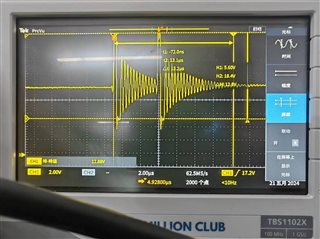
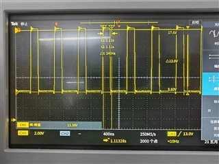
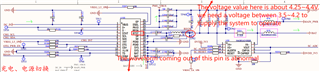
BQ25895M: There is a probability that the PWM waveform on the BTST pin of BQ25895M will be abnormal at the beginning of power-on when there is no battery involved and only using the USB, and the voltage output at the back-end will be higher than the normal value by about 0.1~0.2V, resulting in that the system can not boot up normally.

  • Hello, 

    Thank you for reaching out via E2E. 

    Firstly, can you please help to share a schematic of your design with BQ25895M? 

    voltage output at the back-end will be higher than the normal value by about 0.1~0.2V, resulting in that the system can not boot up normally

    Can you also please help to expand on this statement? What do you mean by back-end? Are you saying the SYS pin output voltage is 0.1 to 0.2V higher than expected? 

    Best Regards,

    Garrett

  • Hello, 

    What is the VREG setting in your system and is charge enabled or disabled in your test? With default register configuration it is not unexpected for SYS to be regulated to approx. 4.4V. in certain operating conditions. 

    Best Regards,

    Garrett 

  • * Created: Tue May 28 10:30:52 CST 2024
    *
    * Format: Register Name  tab Character,\t  Hexadecimal register value.
    * Device: bq25895M
    * BQZ Container: Charger_1_00-bq25895M.bqz
    *
    Input Current Limit, HIZ and ILIM pin	7F
    OTG Temperature thresholds, and Input Voltage DPM Offset	1F
    ADC controls, OTG Frequency, ICO, DCP, and Input Detection	F1
    Battery Load, WDT Reset periods, OTG and Charge Enable, and MINSYS setting	3A
    Fast Charge Current Limit settings and MTK Pump enable	10
    Pre-charge and Termination Current Limit settings	10
    Charge Voltage Regulation Limit, Battery Low Voltage and Recharge threshold	56
    Termination Current Enable, STAT pin, WDT, Safety Timer, and JEITA Charge Current	CD
    IR Compensation and Thermal Regulation thresholds	D3
    ICO, Extended Safety Timer, BATFET control, MTK Pump Voltage, and JEITA Charge Voltage	40
    OTG Regulation Voltage and Current Limit settings	93
    Charger VBUS, Charging Mode, PG, USB Input, and System Voltage Regulation status	7E
    WDT, OTG/VBUS OVP, Thermal Shutdown, Safety Timer, and TS pin faults	00
    Input Voltage DPM settings	23
    Thermal Regulation Charge Status, and ADC Battery Voltage conversion	5C
    ADC System Voltage conversion	5E
    ADC TS pin voltage as percentage of REGN conversion	54
    VBUS status, and ADC VBUS Voltage conversion	E0
    ADC Charge Current conversion	00
    DPM status, and Input Current Limit setting	3F
    Registers reset, Input Current Optimizer status, Device ID, and Temperature Profile	3A
    这是系统完全开机时的寄存器配置,我不确定系统开机不成功时寄存器配置是什么样子的,当我插入 TYP-C 准备捕获时处于不成功的开机状态,系统会从异常状态开机恢复正常;

  • This is the register configuration when the system is fully booted, I'm not sure what the register configuration looks like when the system is unsuccessfully booted, when I plug in the TYP-C ready to capture in an unsuccessful boot state, the system will boot back to normal from an abnormal state;%MCEpastebin%

  • Hi Xien, 

    Understood. Thank you for providing the register configuration on successful boot. 

    In your configuration I see VREG = 4.176V and IR COMP voltage clamp = 128mV meaning bat pin voltage could be as high as 4.304V. If battery is at or near full charge SYS will be regulated above 4.2V. Similarly with default register settings SYS will be regulated above 4.2V when battery is at or near full charge. 

    To further debug any potential issue please help to provide a waveform showing VBUS, VBAT, and VSYS at the time of unsuccessful system boot up.

    Best Regards,

    Garrett

  • Hi 

     for the time being, I have not successfully captured the status information of unsuccessful startup, except for the waveform of BTST pin which may be as described in the question, no obvious anomalies have been found on several other pins, all of which were tested in the battery-less state, and I found that there are some differences in the register configuration of BQ25895M during system startup when I was doing another debugging, the most obvious one being the input limit voltage Different, the nominal application range of 3.6 ~ 14V, the actual use of the 5V adapter can not start the system!

  • Hi Xien, 

    According to the register dump provided the input voltage limit is being set to 4.5V. That should not prevent you from starting the SYS output with a 5V input. The input voltage limit is automatically set following an input plug in. 4.5V setting is expected with a 5V input. 

    Please be aware that when testing with no battery the device must soft-start the SYS output. It is described in section 8.2.3.5 of the datasheet. If you have a larger SYS load than 200mA at startup this would prevent SYS from ramping up to expected voltage level.  x

    Best Regards,

    Garrett

  • Thank you for your answer, this explains one of our startup anomalies, I will continue to debug the issue about the 5V adapter not starting up fully and get back to you with the captured information, hopefully you can give us some suggestions, thanks again!