This thread has been locked.

If you have a related question, please click the "Ask a related question" button in the top right corner. The newly created question will be automatically linked to this question.

PTCH mode to APP mode via I2Ct

Part Number: TPS25751

Hi Team,

I think TPS25751 operating in PTCH mode can't let typeC work(sink&source) SO we need to TPS25751 operate in APP mode. Is it correct? (Question#1)

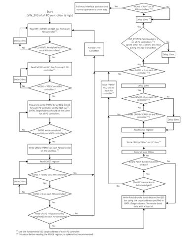
Currently, we don't have EEPROM or EC to configurate the TPS25751 and we try to use micro-controller to send the CMD via I2Ct. We refer to TRM section 5.1. It shows the flow from PTCH mode to APP mode, but it's hard to understand. I find the E2E : https://e2e.ti.com/support/power-management-group/power-management/f/power-management-forum/1345350/tps25751-ptch-mode-update-fails/5131826?tisearch=e2e-sitesearch&keymatch=PTCH%252520OR%252520APP#5131826

And Kevin shows the saleae log. We want to follow the log and let our TPS25751 enter in APP mode.

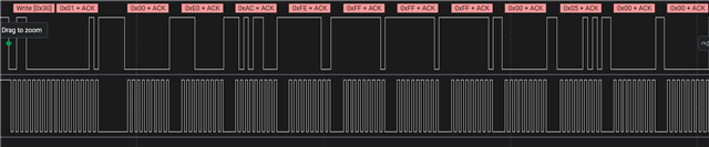
1. It reads 3h register and report the 50 54 43 48 (PTCH) OK

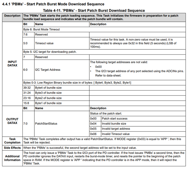
2. It writes 9h(DATA) register, 6bytes, 40 2B  00 00 30 32, what does it mean?(Question#2)

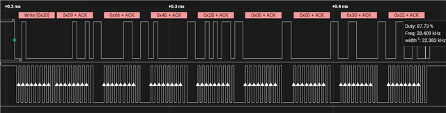
3. It writes 8h(CMD)register, 4bytes, 50 42 4D 73 (Write PBMs) OK

4. It reads 8h(CMD)register, 4byte, and report all "0''. OK

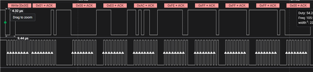
5. it writes 0x30(target  address) 1h register so many registers.

How can I define the target address? In datasheet, it said that defined by ADCINx, but in this log, it used 0x20, but why use 0x30 here? (Question#3)

What does the data mean here? (Question#4)


Regards,

Roy

  • Hi Roy,

    Yes, PD is not enabled in PTCH mode. In PTCH mode, the main firmware of the device is not running. The device must be in APP mode to enable PD.

    1.) This is ok. PTCH mode is required to enable patch loading using PBMx commands.

    2.) Register 0x09 (9h) is the Data1 register for our PD controller's 4CC commands. The Data1 register is loaded with necessary information for PD to execute the 'PBMs' 4CC command in the next step. See command description in TRM below:

    3.) Register 0x08 (8h) is the CMD1 register. Writing 'PBMs' to register 0x08 is ok and will initiate the patch load sequence. The 0x09 Data1 register must be written to before the 'PBMs' command is sent.

    4.) This is ok. Reading all 0s back from the 0x08 CMD1 register indicates that the 'PBMs' command was executed successfully.

    5.) The I2C target address for the patch is different than the typical I2C target address for the PD. This I2C target address for the patch is an arbitrary address that acts as a pointer in memory that the patch data is written to. It is defined in the input to the 0x09 Data1 register in the previous steps. This I2C target address was set arbitrarily to 0x30 in the example. It is expected that the EC or MCU will then write the patch to this I2C target address. You can select any I2C target address that is not the actual I2C address of the PD controller, just make sure it is also set properly in the input data to the 0x09 Data1 register in the previous steps (screenshot above). 

    *The I2C write from the EC to address 0x30 is the patch data, as mentioned in the response to question 5.

    Let me know if you need further clarification.

    Best,

    Alex

  • Hi Alex,

    Thank you for your comments.

    1. For I2C target address, we can set the address that we want, is it correct? 40h 2Bh 00h "30h" 32h. In this case, it select 0x30. 32h is for timeout.

    But how can I define the 40h 2Bh for bundle size?

     It writes 9h(DATA) register, 6bytes, 40 2B  00 00 30 32, what does it mean?(Question#2)

    2. What is the patch data the EC to address 0x30?

    *The I2C write from the EC to address 0x30 is the patch data, as mentioned in the response to question 5.

    I have no idea the meaning of below CMD "Write target address 0x30 about the register 0x01, 00h E0h, ACh, FEh, FFh and so on."

    Does it include in the below flow?

    In addition, may you let me know what is the full name of 4CC? Four characters command?

    If we want to configure the typeC port from DRP to sink only. Do I just need issue 4CC CMD 'SWSk' like PBMs that we issued for mode transition before?(PTCH to APP) (8h(CMD)register, 4bytes, 50 42 4D 73 (Write PBMs))

    What is the different if we issue the 0x28 register [1:0] bit?

    Regards,

    Roy

  • Hi Roy,

    1.) Bundle size is the size in bytes of the entire patch. In the example, the patch size is 0x2B40 or 11072 Bytes. 

    2.) After 'PBMs' is completed, the EC must write the patch contents over I2C. The EC will write the patch contents to the I2C target address chosen in the input data to the 'PBMs' command, in this case address 0x30.

    3.) 4CC means 4 character command. 

    4.) 'SWSk' command will swap the PD's power role from source to sink. This does not change the port's role configuration. On a new connection, PD port will revert to its originally configured role. To change the port's configured role, the EC must write to register 0x28 Port Configuration bits 1:0 to change the "TypeC State Machine" field. This will trigger a disconnect on the port and the port will then have the newly configured role.

    Best,

    Alex

  • Hi Alex,

    Thank you for your comments. Now we can enter in APP mode to do source and sink function. But still has one question would like to check with you.

    For 4CC CMD like 'SWSk', we only to write CMD1 4byte data as my 4CC CMD? No need to issue DATA1 Is it correct?

    Regards,

    Roy

  • Hi Roy,

    Correct. SWSk command does not require any input to Data1 register.

    Best,

    Alex