This thread has been locked.

If you have a related question, please click the "Ask a related question" button in the top right corner. The newly created question will be automatically linked to this question.

LM51501-Q1: LM51501-Q1 - Boost 1.5V ~2.9V to 6.5V@5A

Part Number: LM51501-Q1

Hi, 

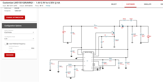
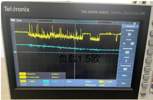
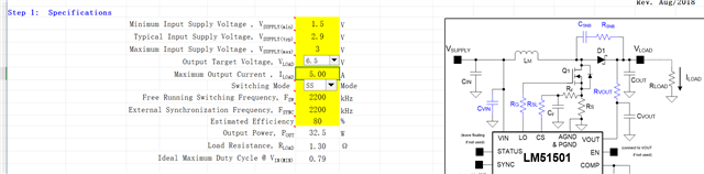
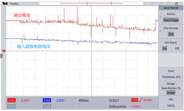
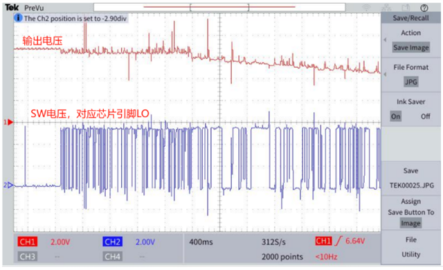
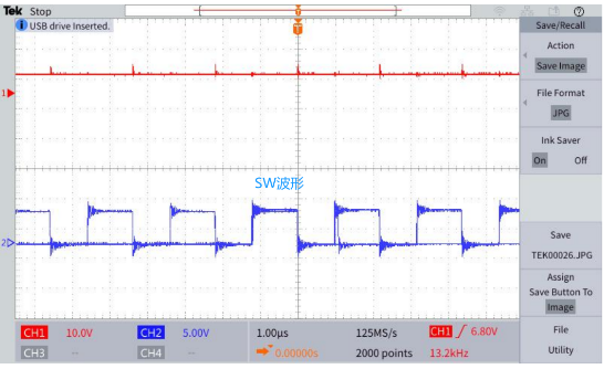
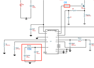
Now,  I use LM51501-Q1 to boost the super-cap, the input voltage is 1.5V~2.9V,  the output is 6.5V@5A according to the value excel form of LM50501 Quick start. I find the output voltage could not be stable to 6.5V@5A, the output voltage will drop to about 4.7V. 

Please help confirm how can I adjust my circuit. 

Thanks a lot! 

Andy

  • Hi Andy,

    Thanks for using the e2e forum.

    I double checked the webench design and also went through the calculator recommendations.
    The design looks valid to me.
    There should be no unintended trigger of the overcurrent protection and the duty cycle is also within the capable limits.
    Compensation should be stable as well.

    Just for clarification, you are running the application with 440kHz fsw, as in the schematic, and not with the 2.2MHz of the calculator screenshot?

    Can you please check the following:

    - Inductor ratings (peak current of 30A is expected, please make sure saturation limits are higher)
    - How does the SW voltage look like during the load transient? Is it oscillating or running with maximum duty cycle?

    Thanks and best regards,
    Niklas

  • Hi Niklas, 

    The frequency is 440KHz and work under ecall mode.  

    After modified the inductor and the relative caps, now the circuit has great improvement. But when the input voltage is under 1.8V, the output will decrease again.  Please find the waveform. 

    Thanks a lot! 

    Andy

  • Hi Andy,

    I am glad to hear there is already an improvement to the original design.

    If the design still has problems during worst case conditions (min Vin, max Load), some additional fine tuning might be required.
    Would you be willing to share the schematic of your design?

    The webench schematic you share is a good starting point, but for fine tuning it would be helpful to know which inductor is used now, what output capacitance, gate resistor, snubber and compensation network is used.

    Thanks and best regards,
    Niklas

  • Hi Niklas, 

    Please find the values in bellow picture. 

    Thanks a lot! 

    Andy

  • Hi Andy,

    Niklas is out of the office but can comment till end of the week.

    Best regards,

     Stefan

  • Hi Stefan, 

    Thanks!

    Add the output cap and inductor info. 

    The load resistor is 1.2Ohm, the output cap is 10uf+330uf*2 +1000uf, inductor is 100nh@60A, sampling resistance 1mΩ, diode 15A, EDLC power supply. 

  • Hi Andy,
    thanks for the additional inputs.

    Best regards,

     Stefan

  • Hi Stefan,

    Another issue, this circuit will be worse under -40°C, what could cause this condition?

    Thanks a lot! 

    Andy

  • Hi Andy,

    Sorry for the delay.
    So inductance has been reduced to 100nH...
    This value is rather small, leading to high current ripple (spikes above 40A at max load would not surprise me)
    Keeping the original inductance of 740nH might result in lower core losses and higher efficiency.

    However, the system should still be able to run stable with 100nH.
    Are you using a slope compensation resistor?
    As duty cycle above 50% is possible at min Vin, there is a risk of subharmonic oscillation.
    This can be avoided by placing a slope compensation resistor at the CS pin.

    Best regards,
    Niklas