Other Parts Discussed in Thread: CSD87313DMS
Hi,
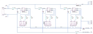
I am implementing a battery protection circuit based on BQ29707 combined with CSD87313DMS. Due to special requirements the BQ29707 is triplicated as in the schematics below. I am experiencing difficulties enabling the FETs in some specific situations. I will describe one hoping to get some advice (questions below).
My device will slowly discharge the battery to 2.8V and then cut the voltage to 0V at pack level (VBATT - GND). So far, so good. Here I refer to 'GND' as the negative pack terminal, while I call the negative cell terminal 'CELL_N' (which connects to VSS of the BQ29707). When I then apply my charger, 3.0V is applied at pack level (VBATT - GND), but the FETs stay in OFF mode. For instance, zero VBATT current is measured through F1. The cell voltage (CELL_P - CELL_N) is measured to a stable 2.8V, so 0.2V below the 3.0V applied at pack level. The only way I found to get it back is to apply >3.5V at pack level with a power supply.
So, I seem to have problems releasing the over-discharge state. To my understanding the BQ29707 should cut at CELL_P - CELL_N = VUVP = 2.8V (as it does) and then release when CELL_P - CELL_N = 2.8 + 100 +/-50 mV hysteresis = max 2.95V. At least if "V– is higher than –0.7 V". If so, I need to ensure that my charger manages to increase the cell voltage by 150 mV to enable the discharge FETs again.
- Question 1: Is my understanding about what makes the discharge FETs turn on correct (that I need up to CELL_P - CELL_N = 2.95V)?
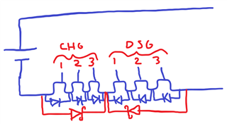
To be able to charge the cell to 2.95V, I assume I need to pass current through enabled charging FETs + the body diodes of a disabled discharging FETs. When I have a over-discharge fault I assume the charging FETs are ON, so it is the CSD87313DMS body diodes I need to handle. Considering room temperature (as a start), the datasheet seems to indicate that current starts to flow at about 0.4V forward voltage.
- Question 2: Do I need to apply 2.8V + 3x 0.4V = 4.0V to pass current to the cell and eventually enable the charging FETs? Or is "V– is lower than –0.7 V" the extreme I need to consider, meaning 2.8 + 0.7 = 3.5V I assume?
- Question 3: Seeing that this "V– is lower than –0.7 V" case is said not to require any hysteresis, is it correct to understand that it does not need to forward bias any body diodes to charge the cell a bit first, it just opens the discharge FET right away?
Both 3.5V and 4.0V are high values since the system would like to boot before reaching that. Then again, it would be due to my odd setup with triplicated FETs, so perhaps I am just reacting because I am used to seeing lower values in typical designs. That would be 2.8 + 0.4 = 3.2V then I assume.
- Question 4: Seeing that the charger tries with 3.0V (which is lower than 3.2V), should I not expect 3.0V to do a good job at disabling the over-discharge fault even in a setup with a single CSD87313DMS, as it is less than 2.8V + 0.4V?
Thank you!