This thread has been locked.

If you have a related question, please click the "Ask a related question" button in the top right corner. The newly created question will be automatically linked to this question.

BQ77910A recovery from OC (Over Current) and SCD (Short circuit discharge)

Other Parts Discussed in Thread: BQ77910A

Dear All,

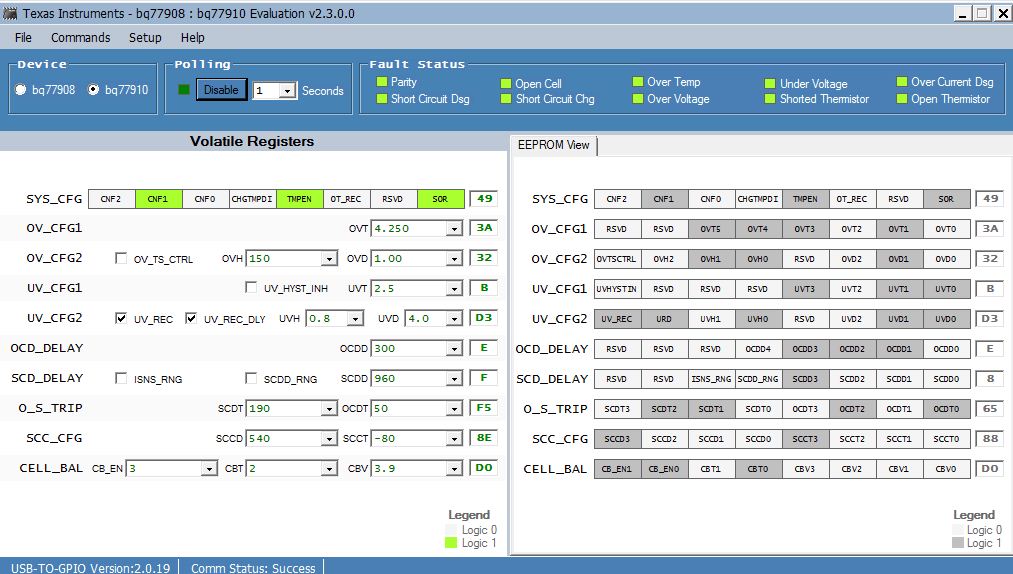
I attached a picture of my CFG file.

my sense resistor is 3 mOhm.

I use a series FET method with the a steady 15K resistor on CHGST.

I set the OC parameter to be around 15A. when reaching 13A the battery cuts off like it should  and removing the load wakes it up.

when reaching 14.5A the battery reacts likewhen in SC (which is wierd as well) -

the discharge FET oscilates, which means the pack closes and opens the current flow until I disconnecting the E load or seperating the short circuit wires.

why does the chip reacts this way on 15A load?

is there a way to have it steady off untill short circuit is removed?

thanks for any help,

  • Hi Ran,

    Your evaluation software screen capture shows some differences between the registers and the EEPROM values. It appears some values were changed but not written to EEPROM. The part operates from the EEPROM.

    You have SOR =1 so overcurrent recover requires both load removal (DPCKN low) and CHGST high.  One thing that can happen in a pack with the bq77910A is that a high capacitive load may not change voltage quickly after OC protection, so DPCKN does not rise quickly and the IC sees load removal too early.  If the pack has a separate CHGST control line, the part may still be prevented from recovering by CHGST low, as you have configured.  If CHGST is high, the IC can see both load removal and CHGST high and recover automatically causing cycling. Higher current such as a definite short circuit usually allows DPCKN to rise faster for more certain load removal, you might check if your load responds slower at higher current though.

    However load present is not a fault and normal operation including wakeup does not require load removal.  If your higher current induces a reset of the part, the FETs turn off.  If CHGST is high or pulses high, the part can start up again and will close the FETs if there are no faults.  This will result in the FETs cycling, but the off time will be the startup time instead of the shorter recovery time.  Causes of reset might include noise coupled onto VREG, noise on ground affecting VREG, or a rapid rate of change on BAT.  See www.ti.com/lit/slua612

    Noise coupled onto ZEDE making the pin momentarily high may also allow the part to go to minimum delay mode and trip without waiting the entire delay time.  Polling as your evaluation software capure shows may also cause cycling if the current is above a threshold or has noise/surges above the threshold.  Polling cycling will show up at the polling interval, although if the load is above the OC threshold may show mostly OCD timing interspersed with shorter ZEDE induced timing.  Since your capture does not show OC faults, you either did not capture during cycling or do not poll durig cycling.

    So in general:

    • Be sure it is a protection and not a reset
    • Check for transients on control lines
    • Check to see if load detection is 'high', load detection can be before protection.
    • Best IC functionality is if CHGST is controlled (indicates charger is connected)
    • No status polling during test


  • Dear WM5295,

    thanks for your answers,

    1. how can I check if it is a protection or reset, since I can't use polling?
    2. if it is DPCKN rising to slow, how can I make sure it will go faster for the currnet I'm interesting in - up to 15A? should I increace/decrease C29/R46 ?

    schematics is attached,

    thanks again,

    Ran Aloni

    Schematic_B4.pdf
  • If you use polling you may induce errors.  If your error is static, you can poll after the error to see what one(s).  Reading may still induce a new error, but if the underlying error is repeatable, the induced errors will likely show as such with a few trials.  If the error is dynamic with FETs cycling as you described, it is more challenging.

    • You could check for polling induced faults with a scope on ZEDE and DSG for example.  If DSG falls when ZEDE is high, it was likely induced by zero delay mode.
    • If you are polling at 1s and the fault occurs faster, it is not likely polling
    • If it recovers ~ 100ms after the event, it is likely a reset and power up event (see figure 5 in the datasheet)
    • If it recovers in <<100 ms, it is likely a failure to see the load detection

    The part only allows ~ 100us for DPCKN go get above the threshold before it starts recovery. You can adjust C29 to make it faster, just be sure it keeps any overshoot at protection within abs max limits.  R46 is to aid self recovery from a loaded fault condition as described in the datasheet.  If placing the pack in the charger to recover is suitable, you do not need R46   If pack- does not move at fault, using the CHGST signal high from a charger for recovery is an option, but not for your schematic.  So it gets complicated as you need to control one of those signals.  Since DPCKN low is not a condition to startup, you can pull DPCKN up until you want to recover after a fault, then use some mechanism to pull it low such as a certain pack voltage conditon or a signal derived from a pack pushbutton.

     Since you hare holding CHGST high at all times, you may consider making R33 and R34 larger to reduce quiescent current.  Just don't make them so large that CHGST switches with noise.

  • Dear WM5295,

    C29 is currently 0.1uF.
    I assume that I should replace it with a smaller capacitor to make DPCKN react faster than the recovery.

    how effectively small can I make C29?

    as for now the Battery does not pass a UN test. which is very severe...

    since uControler is not an option here to keep DPCKN high while load is connected, what can I do except replacing C29?

    will rmoving R46 make things faster as well?

    your urgent assistance is most welcome.

  • Reducing C29 can allow DPCKN to move faster.  C29 is in the circuit to prevent inductive spikes on P- from reaching the DPCKN pin and causing damage.  C29 could be replaced by a zener or TVS clamp or eliminated if your systen has no overshoot on P-.  R46 is large enough that it likely will have little effect on the response speed.  If P- does not move fast enough to allow DPCKN to rise to prevent the part from automatically recovering, you will need some other circuitry to signal it.

    One solution may be to bias DPCKN closer to the load detection/recovery threshold so that P- does ot have to move much.  This can result in undesired bias current and possibly increase leakage while the pack is in fault.  It will still be difficult to do if P- moves slowly.

    The part needs some signal to indicate when to recover.  The 2 options are CHGST and DPCKN.  If you have a CHGST signal, that may be an option but it appears fixed in your design.  If P- and thus DPCKN does not move fast enough, adding some circuit to DPCKN which can signal the part to recover will be needed.

    One option may be to hold DPCKN up above the load detection/recovery threshold most times.  After an OCD/SCD event this will prevent the part from recovering until you signal it.  Note that load removal is not a condition to wake the part or a fault itself, so that is OK.  Do be sure to look at your UV recovery settings where load detection can also be used.  DPCKN might be pulled up to VREG for example through a resistor & diode.  To signal the part to recover from an OC event, you would need some signal.  Perhaps that is a capacitvely coupled connection to P- so that when the P- moves from P+ to normal by the applicaiton of a charger for example, the circuit responds fast enough to pull DPCKN down below the threshold and recover.  This requires a specific behavior of the system to work.  Another may be a FET or 2 to turn on and pull DPCKN down when the charger voltage exceeds the battery voltage.  This again requires a specific system behavior.  Those solutions may require additional clamp diodes to prevent DPCKN from going too high or too negative due to the coupling.  A third signal option may be the user pressing the switch to initiate DPCKN low and current recovery.  That might be done with a signal FET, but would require specific user behavior.

    Beyond these it seems you need a sequential circuit which recognizes that  P- goes higher than some threshold, then waits until after it falls below another threshold to attempt recovery by pulling DPCKN low.


  • Dear WM5295,

    We do appreciate your help,

    I tried to use C29 as 0.01uF, and still reacts about the same. this is a bit of a problem since we are out with 500 pcs we want to use.

    1)just to verify: C29 , according to the EVM schematics is between DPCKN and B-, not P-.

    2) if I understand correctly the zener/TVS you suggested between DPCKN and B-, should be above 40V since the voltage over DPCKN can reach around VBAT which can be ~34V. do you think it is relevant after the very small capacitor that didn't work?

    3) you mentioned a solution with pulling up DPCKN with  a diode/res to VREG permanently.
    while in a condition (OC,UV), how can I pull it back down when load is disconnected? (a button is not an option). can you suggest a simple AN to tie DPCKN to ground when load is disconnected?

    4) which system behavior for DPCKN to be pulled up all the time? since my CHGST is pulled up at all time (series FET topology) it won't recover ever if my SOR=1 and wil recover always when my SOR =0, right?

    thanks again - we are in a very crucial phase.

  • 1. Yes, DPCKN's (abs max) limit is with respect to VSS or B-.

    2. A zener or TVS capacitance may be much less than 0.01uF.  This is likely the lowest component count change, but if P- or the common drain point where R45 connects is not moving very fast, the smaller capacitance may not help.  If P- is moving but the common drain point is not, you might be able to move the detection point to P- with sufficient clamping to protect DPCKN.

    3. Attached is a concept, not a tested circuit.  It may or may not work.  Consider it with other options you may have.  It might be done in some simpler way.1538.Concept1.pdf

    The pullup source is from some voltage above the VOPEN_LOAD threshold. VREG at 3.3V is above the VOPEN_LOAD threshold but does not give much headroom.  DCAP is ~ 12V when pack voltage is sufficient and provides more headroom, but its current should be very low and the higher voltage will also require more signal swing to cross the threshold & recover.  If your schematic's 15V is available, that may be an option.

    D1 blocks the circuit from driving current back into the source.  If using VREG this may need to be a schottky due to the small headroom.

    R1 provides the pull up.  It will make a voltage divider with the internal IC pull down, or R46 if you retain that.  You would like this to be large so that your quiescent current is small and the circuit recovery does not pull down the source such as inducing a reset if VREG is used.

    R2 limits current into the DPCKN pin.  It might be the 100 ohm of your R45 (datasheet RDPCKN)

    D2 and D3 limit the voltage to the DPCKN pin to keep it within abs max limits.  The D2 forward voltage may be high enough a D3 schottky is needed when NET1 goes below GND.  With C1 the body diode of the discharge FET does not limit the voltage.

    C1 pulls the NET1 node and DPCKN up or down as P- swings. You want it large enough to get a transition across the threshold on fall of P-.  Note that P- must swing at some definite rate for this to work.  If it drifts slowly C1 may charge/discharge without moving NET1 significantly.

    R3 limits the current into the diodes and will influence the response time.

    If the charger won't provide a definite swing  of the P- signal, a DC circuit may be driven from a detector like Q19 and Q20 of www.ti.com/lit/slua637.  The Q19 drain signal could be used to turn on a FET to pull down the DPCKN. Again this requires a specific system behavior of P- going below B- to actuate. 

    4. Refering to table 2 of the datasheet, with CHGST always high, SOR seems like a don't care condition because current fault recovery will depend on load removal sensed by DPCKN.  The other apparent considerations are undervoltage and OT recovery.  With CHGST high the CHG output will come on/stay on.  You may want UV_REC =0 and TMP_REC=0 so load removal is not needed, or use the same recovery mechanism as for current protection recovery.

    Always test thoroughly.

  • Dear WM5295,

    thanks for your replys,

    I took some measures to isolate the problem. I wanted to see that when the DPCKN pin is over 2V the problem is solved.

    1)I disconnected R46 and R45 - to isolate the common drain.

    2) I connected DPCKN to Vreg (3.3V) via a schottky diode (0.2V drop) to keep it high and over 2V.

    as I expected, after applying 20A load, the circuit was cut off, and removal of load had no effect.
    but the problem of FET oscilation is still there...

    you can really here the FETs ticking - they are not steady off.

    that is the real problem, because it allows peaks of current to flow through the circuit.

    what happens when we manually short circuit the battery is randomly one of the balancing resistor gets burnt.

    so the problem is not the DPCKN in my eyes, since they did not wake up the event this time, and obviously not CHGST.

    I attached the FETs datasheet to be sure.

    any ideas?

    so what causes the FET oscilation.

    AP94T07GH,J-HF (20110428).PDF
  • The description and test with DPCKN high seem to indicate it is not a fault recovery, but most likely reset.  With the clicking slow enough to be heard and not a constant buzz, it is very likely a reset and the longer start up delay time of the part.  Please see the posts above and www.ti.com/lit/slua612

    The current from the battery with a manual short can be very high and the fast turn off of the FET can excite the cell inductance and produce a high voltage spike.  The pack level clamp of D7 still has a resistive characteristic and the voltage can rise past the nominal value. If the cell input voltages at the IC exceed the abs max of an input pin it can cause a short circuit of the input to ground.  The resulting high current through the balance resistor causes it to burn.  Depending on the resulting voltages, adjacent inputs may be damaged also. If you can slow down the switching speed by increasing your R41 the current cut off will be slower and the voltage transient smaller.  Do not violate the safe operating area of your FET however.  Increasing the filter resistance some (which also reduces balance current) may help, but you may need to clamp the input pins.  See the EVM user guide www.ti.com/lit/sluu855 . The EVM used a clamp at the top input pin and one on VC7 which showed to be more sensitive than others, D18 and D12 (or in an 8 cell case D18 and D14).  Some users report damaging VC10, but more often during cell connection.  VC10 is more difficult to clamp due to the balancing voltage swing and it may be easier to clamp the bottom cell voltage if needed.

  • Dear WM5295,

    thanks for the fast replys,
    we want the BQ77910A to work for us, we are counting on it for more designs, but the currents will be about the same as here, so we have to solve this problem, which seems to be non related to the fact we are using Series FET method is it?

    1)I place a scope (10ms samples) on the VREG while the oscilations happens, and it doen't seem to crash. is this because of the high CHGST?
    2) couldn't measure VBAT (out of my scope scale) what is happening there..

    3) one issue, as far as I see it, I have no interest in better protecting VC7 or VC10, since this takes care of the results of the oscilations, I want to stop these oscilations from ever happening...

    4) I know this manual, what specifically is relevant for me there? since a big chunck of it takes care of transient currents, and I only use an ideal E load at this moment, I do not expect transients at all...

    5) why do you think my chip resets every 1s or so when going over 15A?
    problem is less harsh when I strngtht the parameters. meaning: I defined the OCD to be 10A and SCD to be 15A, but when manually SC the pack it reacted the same... still not acceptable by UN testing.

    do you need more information from me?
    anything more I can send? I couldn't send the *.PCB file over the forum attachements.

    best regards,

  • I know the frustration.  As you indicate the currents will be the same for series or parallel configuration.  With series configuration the transients will feed into the part not only through the cells and the normal BAT feed path, but also from CPCKN as it flies up with P- and the CHG driver becomes a diode into BAT.  This has the potential to break the CHG driver, which you fortunately do not have, or make BAT rise suddenly which can reset the part.  CPCKN will feed into BAT inside the package.  Since it is a discharge event you might consider a modification of a board to separate the CHG and CPCKN from the FET and temporarily ground CPCKN to VSS and power the charge FET with a 9V battery or short it. See if the oscillation effect is changed.  Be sure to make the pack safe again for charge after the test.

    Since you mention UN testing you apparently have a system issue (all packs behave the same) and not a single bad unit. Your DPCKN experiment seems to confirm it is not a immediate recovery, so it would seem to be a likely reset.


    1. Correct.  If CHGST was low and there was a reset, VREG would fall slowly. Since CHGST is high, as soon as VREG falls to POR, it sees CHGST high and wakes up again.  It may be hard to see the drop in VREG which may be in the 10's of us, but the logic will go through the wake up sequence.  You should be able to see some duration of DSG off which looks like the start up time from figure 5.

    You might try triggering on the falling edge of DSG and looking in detail at VREG.  Note the VPOR parameter in the datasheet, it only has to dip below 2.7 to have a reset.  You might also try disconnecting CHGST on a pack after it is awake before applying the 20A.  See if VREG falls and it stays off, or if it is some unexpected recovery.

    2. You might try connecting to BAT with a capacitor to block the DC.  You can extend the range of the probe with a series resistor to change the divider ration, but this will reduce the bandwidth also.

    Another approach is to try to prevent it without seeing it.  You might try adding capacitance at the IC pins or moving the capacitor to the pin.  This might also be good for VREG.  A second inspection of your layout as you suggest could be good to check for unexpected currents through your ground, long routes to the capacitors or large loops which could couple in noise.

    3. That is a good point, getting rid of the transient would make all else easier.  From the cell voltage or voltage input into the IC's circuit, when you switch the current you add in a voltage V = L x dI/dt. 

    L is a characteristic of the cells, perhaps around 0.3uH/cell. The interconnect may add some also, but ignore it if possible.

    dI is the change in current, which may be the E-load setting, or in the case of the manual short or the UN test short, as much as the cells can produce, perhaps in the 80 to 150A range.

    dt for the protection event is the switching off time of the discharge FET.  This will depend on the '910A DSG switching speed (which is fast), the DSG series resistor (R41), the discharge FET gate capacitance and the FET's threshold voltage.

    So for 20A with 5 us switching, your voltage step might be .3x20/5 or about 1.2V, which is not too bad.  The cell may not be heavily loaded and the voltage might not drop much with the load or recover, so you may see 4V to 5.2V per cell change.

    If you have 100A switching with the short in the same 5us, you would have .3x100/5 or 6V step.  A 4V cell may have pulled to near 0V during the short, so it recovers when the load is removed and each cell sees a momentary 9-10V step.  This is harder to keep out of the inputs. The larger step with the manual short may be why the balance resistors burn. 5 us is likely faster than the switching, so transients may not be so large, but the concept applies.

    To eliminate or reduce the impulse, the easiest thing to control is the dt by adjusting the series resistor R41. However too large and the FET switching is too slow - the FET can fail, usually shorted.  Use a fuse in your test short if you are pushing the safe operating area of the FET.

     4. Unfortunately it is all related. The signals wrap around the part.  The transients are not particularly from the E-load although that may affect CPCKN and through CPCKN to the BAT pin.

    5. I would expect a reset induced somehow by the SCD protection, but that would not normally line up with 1s.  The oscillation time may be very significant to determine the fault that is causing the event. The SCD time selection looks like ~ 1ms and a 100 ms startup delay should give a must faster cycle.  Unless your configuration changed significantly, only the OV looks like a 1s delay and it is hard to envision an OV induced by current.

    ZEDE is a high impedance input and has a high 100k pull-down. Our system engineers would like to see more like 1k pull-down.  If this were to trigger, the part could protect from having crossed the OCD threshold, but any oscillation should have been stopped by your DPCKN experiment, and there is no clear trigger for the ZEDE event; it still seems like a reset.

    The layout may be a good place to look.  You should be able to look at it with a colleague.  Key items would include to be sure load current does not flow in the ground reference for the chip moving the VSS pins from each other, BAT and VREF capacitors close to the IC and away from the current path, and avoiding loops that the current could couple into.

    Pins pushed below VSS can cause an IC to reset, but there is no apparent reason for it to delay from the application of the current.

    Unfortunately it is a phenomena you will need to measure some fault & fix, or add/change component placement until it is fixed or you see a change which leads to a fix.


  • Dear WM5295,

    I had a small change of approach,

    I have a gas gauge on the circuit that is connected to B+ through a tactical switch.

    basically I connected B+ through the tactical switch to CHGST.
    as I chose SOR = 1, the curcuit will only recover if I disconnect the load and press the button.

    I would expected the chip to go to sleep while appline the high currents and short circuit...

    but why does it go off and on?
    Vreg is oscilating in 300 ms (see attached scope pictures in ZIP)

    I would expect it to stay off since it doesn't wake up on charge...


    VREG scope.zip
  • Dear WM5295,

    I examined your comment about the voltage over Vgs.
    that seems to be the problem!

    I replaced R41 and R48 to 2 x 200K resistors. which placing a steady ~6V on Vgs.

    this is a solution for this pack (although a bit current wasting), I guess a simple 5.6V Zener would have been in order if I had more freedom for changes at this point.

    you really have to refer to that in the application notes, since this is a classic E bike chip that should handle these currents.
    I connected the CHGST to B+ (through 15K) again to minimize changed in production.

    further testing to be made, I will keep you posted.

    thanks a lot for your help until now.

  • Glad you found it.  It should not be the Vgs while on that is the issue, but the speed of turn off.

    The DSG output is a roughly regulated (12V) signal within the Vgs range of common power FETs.

    R48 and R41 in parallel will discharge the FET gate capacitance when the DSG goes low. When DSG is high they form a voltage divider to the gate.

    R48 should be able to stay large to hold the gate down while the part is off.  With it large, it has little effect on load current and provides little help in turning the FET off during load.

    R41 would be expected to be the smaller resistor to have the most influence, When DSG is high this would give most of the DSG output voltage to turn on the FET; when DSG goes low it provides the primary discharge path for the gate capacitance and thus controls the switching speed.

    100k (the parallel combination of R41 and R48 at 200k) seems rather large.  Be sure it is switching fast enough for your FET while keeping the transient down.