


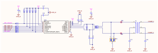
Other Parts Discussed in Thread: BQ79616-Q1, BQ79616
Tool/software:
case 0xF0://Initializes the wake pulse pin
GPIOA_PDDR |= (1 << ePIN_D1); /*MOSI,PTD1*/
GPIOA_PDDR |= (1 << ePIN_D3); /*BQ79600_CS,PTD3*/
GPIOA_BASE_PTR->PDOR |= (1 << 27);/*BQ79600_CS,high*/
GPIOA_BASE_PTR->PDOR |= (1 << 25);/*MOSI as the WAKE pin,high*/
sState = 0xF1;
BSPCosStart(COS_ID_CELL_SAMP, 1);//wait1ms
break;
case 0xF1://Wake pulse timing
GPIOA_BASE_PTR->PDOR &= ~(1 << 27);/*BQ79600_CS,low*/
BSPDelay(3);//delay2us
GPIOA_BASE_PTR->PDOR &= ~(1 << 25);/*MOSI as the WAKE pin,low/
BSPDelay(7500);//delay2.75ms
GPIOA_BASE_PTR->PDOR |= (1 << 25);/*MOSI as the WAKE pin,high*/
BSPDelay(3);//delay2us
GPIOA_BASE_PTR->PDOR |= (1 << 27);/*BQ79600_CS,high/
sState = 0xff;
BSPCosStart(COS_ID_CELL_SAMP, 10);//wait 10ms
break;
case 0xFF:
BSPSPIInit(eSPI1); //Initializes theSPI
sState = 0x00;
BSPCosStart(COS_ID_CELL_SAMP, 2);
break;
//INITIALIZE BQ79616-Q1 STACK
case 0:
SpiWriteReg(0, CONTROL1, 0x20, 1, FRMWRT_SGL_W); //send wake tone to stack devices
sState = 0x19;//Next automatic addressing timing
BSPCosStart(COS_ID_CELL_SAMP, 12);//wake tone duration is ~1.6ms per board + 10ms per board for each device to wake up from shutdown = 11.6ms per 616 board
break;
//************************
//WRITE AND READ FUNCTIONS
//************************
int SpiWriteReg(BYTE bID, u16 wAddr, uint64 dwData, BYTE bLen, BYTE bWriteType) {
// device address, register start address, data bytes, data length, write type (single, broadcast, stack)
u16 waitTime = 0;
bRes = 0;
memset(spiBuf,0,sizeof(spiBuf));
// while(gioGetBit(gioPORTA, 1) == 0) delayus(5); //wait until SPI_RDY is ready
while(0 == DEVGPIOGetInPortState(ePIn_BQ79616_RDY))
{
waitTime++;
//BSPDelay(5);
if(waitTime > 3000)
{
waitTime = 0;
break;
}
}
switch (bLen) {
case 1:
spiBuf[0] = dwData & 0x00000000000000FF;
bRes = SpiWriteFrame(bID, wAddr, spiBuf, 1, bWriteType);
break;
case 2:
spiBuf[0] = (dwData & 0x000000000000FF00) >> 8;
spiBuf[1] = dwData & 0x00000000000000FF;
bRes = SpiWriteFrame(bID, wAddr, spiBuf, 2, bWriteType);
break;
case 3:
spiBuf[0] = (dwData & 0x0000000000FF0000) >> 16;
spiBuf[1] = (dwData & 0x000000000000FF00) >> 8;
spiBuf[2] = dwData & 0x00000000000000FF;
bRes = SpiWriteFrame(bID, wAddr, spiBuf, 3, bWriteType);
break;
case 4:
spiBuf[0] = (dwData & 0x00000000FF000000) >> 24;
spiBuf[1] = (dwData & 0x0000000000FF0000) >> 16;
spiBuf[2] = (dwData & 0x000000000000FF00) >> 8;
spiBuf[3] = dwData & 0x00000000000000FF;
bRes = SpiWriteFrame(bID, wAddr, spiBuf, 4, bWriteType);
break;
case 5:
spiBuf[0] = (dwData & 0x000000FF00000000) >> 32;
spiBuf[1] = (dwData & 0x00000000FF000000) >> 24;
spiBuf[2] = (dwData & 0x0000000000FF0000) >> 16;
spiBuf[3] = (dwData & 0x000000000000FF00) >> 8;
spiBuf[4] = dwData & 0x00000000000000FF;
bRes = SpiWriteFrame(bID, wAddr, spiBuf, 5, bWriteType);
break;
case 6:
spiBuf[0] = (dwData & 0x0000FF0000000000) >> 40;
spiBuf[1] = (dwData & 0x000000FF00000000) >> 32;
spiBuf[2] = (dwData & 0x00000000FF000000) >> 24;
spiBuf[3] = (dwData & 0x0000000000FF0000) >> 16;
spiBuf[4] = (dwData & 0x000000000000FF00) >> 8;
spiBuf[5] = dwData & 0x00000000000000FF;
bRes = SpiWriteFrame(bID, wAddr, spiBuf, 6, bWriteType);
break;
case 7:
spiBuf[0] = (dwData & 0x00FF000000000000) >> 48;
spiBuf[1] = (dwData & 0x0000FF0000000000) >> 40;
spiBuf[2] = (dwData & 0x000000FF00000000) >> 32;
spiBuf[3] = (dwData & 0x00000000FF000000) >> 24;
spiBuf[4] = (dwData & 0x0000000000FF0000) >> 16;
spiBuf[5] = (dwData & 0x000000000000FF00) >> 8;
spiBuf[6] = dwData & 0x00000000000000FF;
bRes = SpiWriteFrame(bID, wAddr, spiBuf, 7, bWriteType);
break;
case 8:
spiBuf[0] = (dwData & 0xFF00000000000000) >> 56;
spiBuf[1] = (dwData & 0x00FF000000000000) >> 48;
spiBuf[2] = (dwData & 0x0000FF0000000000) >> 40;
spiBuf[3] = (dwData & 0x000000FF00000000) >> 32;
spiBuf[4] = (dwData & 0x00000000FF000000) >> 24;
spiBuf[5] = (dwData & 0x0000000000FF0000) >> 16;
spiBuf[6] = (dwData & 0x000000000000FF00) >> 8;
spiBuf[7] = dwData & 0x00000000000000FF;
bRes = SpiWriteFrame(bID, wAddr, spiBuf, 8, bWriteType);
break;
default:
break;
}
return bRes;
}
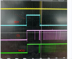
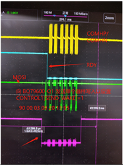
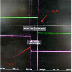
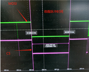
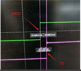
The above picture is the pulse timing of my wake up 600, the time is in line with the requirements, but the oscilloscope measurement in operation SpiWriteReg(0, CONTROL1, 0x20, 1, FRMWRT_SGL_W); //send wake tone to stack devices before RDY is lowered, according to the instructions in the user manual, RDY is lowered, the host write operation to 600 is invalid, would you please help TI engineers to find out the reason?
