Other Parts Discussed in Thread: LM51561H, LM51561, LM5156
Tool/software:
Hello all
What is the Overload current of the part LM5156HEVM-FLY Evaluation Module?
i.e Output overload protection current of the same part
Regards
Aditya
This thread has been locked.
If you have a related question, please click the "Ask a related question" button in the top right corner. The newly created question will be automatically linked to this question.
Tool/software:
Hello all
What is the Overload current of the part LM5156HEVM-FLY Evaluation Module?
i.e Output overload protection current of the same part
Regards
Aditya
Hi Aditya,
Thanks for using E2E.
The maximum output current of the LM5156HEVM-Fly is 4A.
The current limit will be triggered slightly above, depending on the input voltage.
If you have further questions, please feel free to ask.
Best regards,
Moritz
Hello Moritz
Thank you for the Reply
We designed PSU with LM51561H for 5V ,3A
while testing we observed Some Error Can You please help us to resolve.
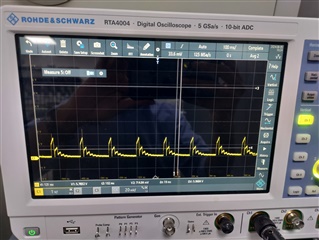
Error - when we increase the current above 3A it goes in Overload protection and it's trying to recover. Observed Output waveform
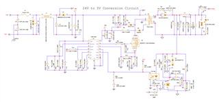
Here is the Attached Schimatic and Output waveforms After goes in Overload protection
Please explain the problem and solution of the same
Regards
Aditya
Hi Aditya,
For reviewing the flyback design, could you please fill in the quickstart calculator and attach it?
https://www.ti.com/tool/download/SNVC240
Thanks and best regards,
Niklas
Hello Niklas
Thank you for reply
PFA QuickStart calculated Sheet
1. One more point: For overload protection, we are achieving a hysteresis as described below. We are attaining overload protection at 4A with a recovery threshold of 3.4A, resulting in a hysteresis of 600mA for recovery
2. We observed the output waveforms of the evaluation board after overload and found that they were the same as those observed in my design.
can you please suggest what is the problem and solution for the same.
Copy of LM5155_56_Excel_Quickstart_Calculator_for_Flyback_Regulator_Design.xlsx
Thanks
Aditya
Hi Aditya,
Thanks for attaching the calculator.
The recommended sense resistance is 25.6mOhm and this design uses a 27mOhm resistor, so I would say there is no issue from this part of the schematic.
Hiccup mode is defined to wait for 32768 pulses between startups. At 250kHz, this would lead to an off-time of ~131ms. This matches with the waveform picture you attached, so I agree this looks like hiccup mode operation.
As the output voltage never reached the target voltage, I would assume this might be related to the softstart.
During startup, all output caps will be charged which adds to the load conditions.
The schematic shows that a secondary side softstart is implemented, but I am afraid that the softstart ramp is still too steep and OCP is triggered.
Due to low resultion, I cannot fully read the output cap values. It looks like values of 820MF. Would that mean the cap has 0.8F, this capacitor would be huge and a very long softstart time would be necessary.
I would recommend to try increasing the softstart time to avoid OCP trigger during startup.
A useful app note on this can be found here:
https://www.ti.com/lit/an/snvaa44/snvaa44.pdf
Best regards,
Niklas
Hello Niklas,
Thank you for the Reply
yes, in my design i am using CLC filter (C-820mF 6.3V, L-10UH, C-820MF 6.3V) because we need Output ripple below 20mV
Could you please suggest is that value ok to use?
Regards
Aditya
Hi Aditya,
Even though a overall capacitance of 1,6F is unusually high for such an application, is it feasible.
To avoid running into OCP during startup, the additional BJT at SS and COMP is important to avoid that COMP signal goes up to quickly.
Right now they are using LM51561 with hiccup feature enable.
If they switch to the non-hiccup version LM5156, the could achieve a full ramp up to the 5V output voltage even though OCP is still triggered.
Then they will lose the hiccup feature though.
If the main goal of the large capacitance is too achieve low output voltage ripple, a cheaper option could be to regulate the output rail to 5.2V and then use an LDO to regulate down to 5V with minimal voltage ripple.
Best regards,
Niklas
Hello Niklas
Thank you for the reply
I got another observation for below test condition
Test condition:
Input- 18VDC
Load - changing the load OA to 3A suddenly
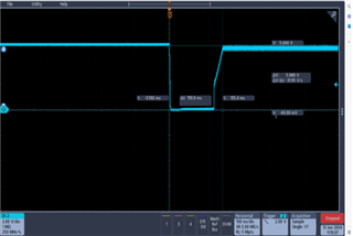
result: observed Output voltage dip 5v to 0v for 160mS
Till 2.7A we do not observe dip. only above 2.7A we observed dip
Attached Waveforms for your reference
Why are we getting Such Dip?
Regards
Aditya
Hi Aditya,
Thanks for the update.
This dip might be related to the hiccup function of LM51561.
If current requirements overshoot to compensate the load transient, it might be possible OCP got triggered and caused the device to enter hiccup mode.
After one hiccup cycle, the device starts with softstart, which limits the inrush current and therefore does not trigger OCP again.
Best regards,
Niklas
Hello niklas
Thank You for the Replay
In my schematic i took feedback before L (10UF inductor).
So, we removed The Inductor (L) and shorted with lead with this case we haven't observed Dip.
Can You please explain why it is happening because Of L filter?
Please Suggest what should i do for this.
Regards
Thank you
Hi Aditya,
It is interesting that removing the filter inductor solved the issue.
I can confirm that it is possible that the output filter can influence the regulation loop. E.g. another customer experience stability issues as they connected their feedback after the filter inductor.
However, this design has the feedback signal taken before the inductor, so an influence on the loop compensation might not necessarily be the case.
It could be possible that the filter inductor changed the form of the load transient itself, which could have led to an overshoot which eventually triggered the OCP, but I cannot be sure about this theory with the information I have right now.
If it is possible to measure the output current waveform with and without the inductor populated, we might get a better picture of the behavior.
Best regards,
Niklas
Hi Aditya,
Yes, load current.
My theory is that the load transient curve looks different with and without the filter placed.
E.g. if the transient slope gets steeper or overshoot, it would be an explanation why OCP got triggered in this situation.
Best regards,
Niklas
Hello Niklas
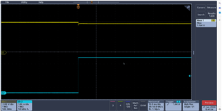
Please find the attachment as requested
Load Voltage and Load current
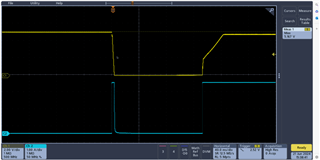
Can you Please suggest how should I correct this issue?
Same Dip I observed In Evolution Board for below condition.
At input -18V DC
Load - 0 to 4.8A
At 18V OCP Of Evalution board is 5A
Regards
Aditya
Hi Aditya,
please give us some time until beginning of next week.
Thanks and best regards,
Moritz
Hi Aditya,
Sorry for the delay due to my absence.
Based on the two waveform pictures, the two loadsteps look identical. At at timescale of 40ms/div, it is difficult to say if the slope of one ramp is steeper than the other one. For this, it would be required to zoom in on both curves.
If it turns out that the load steps is exactly at the corner of triggering OCP for 64 cycle, there are two options to avoid triggering hiccup without switching to the LM5156 version without hiccup feature:
1: reduce sense resistance. This will allow for higher peak currents
2: increase phase margin of the loop compensation. This will damp the reaction to the load transient
Best regards,
Niklas
Hii Niklas
Thank you for the Solutions
Could you please explain briefly?
How should I increase the phase margin of the loop compensation?
Regards
Aditya
Hi Aditya,
The compensation can be calculated by using the quickstart tool I mentioned in a previous reply.
https://www.ti.com/lit/an/snvaa44/snvaa44.pdf
The impact of changing the compensation values can be directly seen in the bode plot.
(Please make sure parameters for output capacitance, inductance and Vin/Vout/Iout are entered correctly)
We normally recommend 60 degree phase margin minimum.
Best regards,
Niklas