This thread has been locked.

If you have a related question, please click the "Ask a related question" button in the top right corner. The newly created question will be automatically linked to this question.

LM5122: Device Damage after power-up

Part Number: LM5122

Tool/software:

Hello,

we have a booster design with the LM5122 and we get some damaged devices after ATP. The feeding supply during ATP provides 20V with a current limit set point of 3A. The fails occured immediately after power-up. The PSU has the following design data:

- Vout = 66V at max. 0.8A (ca. 50W output power)

- Vin = 18-33V (28V typical)

- switching frequency is ca. 210kHz.

- Primary current limit set point ca. 5A via sense resistor (0R015).

Design works principle ok. However, when supplied with lab supply with current limit set point at 3A so well below the current limit of the DUT (5A) then we have the issue that the PSU cannot normally start since input voltage drops. This behaviour is ok. The issue is that for some units the power components fail (low side switch MOSFET) as well as PWM controller (LM5122).PWM controller failure mode and effects seems to be different. Sometimes there is a short between SW node to AGND. Another effect is the short of VCC pin to ground.

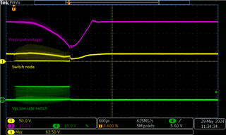
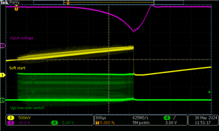
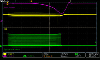
I have measured startup for this scenario (Vin=20V, 3A current limit set point) and seen that sometimes the Low side ON time is quite long, which I don't understand (see screenshots below)

First complete sequence from power-up until first switch if UVLO threshold reached due to too low current limit set point of feeding supply..

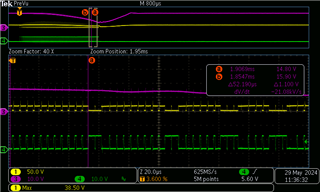
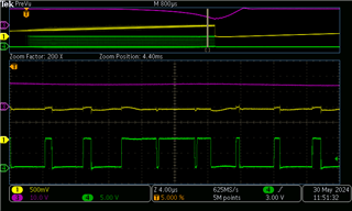
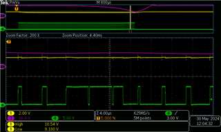
Next figure: the detail for normal switching. It shall be noted that the pulse width increases with time

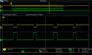
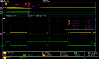
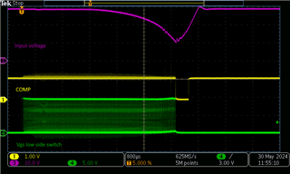
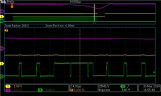
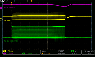
The next figure: detail with unusal long pulse width:

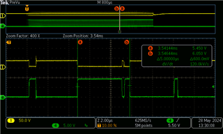
Please note I have switched off channel 3 for the detailed screenshoots (2-3) in order to focus on the most important signals.

First of all the period time is longer than normally, Second there is a short Off-pulse. Input voltage at this zoom area has not dropped. Actually under this scenario I could not catch a damage case. Nevertheless I have the following questions:

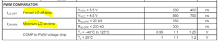
Q1: What are the minimum and maximum pulse width the LM5122 generates during start-up (voltage ramp-up phase)?

Q2: What could cause the unusual long ON pulse shown in last screenshot?

Q3: Is it possible that the LM5122 internal logic / state machine may get stucked and control the Low side MOSFET permanentely ON

For sure, the start-up shall be done with apppropriate current limit of feeding supply. However, I would never expect a device failure (PWM controller itself or one of the switch MOSFETs).

Thanks in advance!

Best Regards Andreas

  • Hi Andreas,

    Thanks for using the e2e forum and describing the problem in detail.

    As you already mentioned yourself, limiting the supply current lower than the peak inductor current limit of the device can lead to a failed start-up, when the application needs to support both the load and charge the output capacitors. If Vin drops, the boost ratio becomes larger, leading higher duty cycle and more input current, making Vin drop even more, and so on until UVLO triggers.

    As for the long low side pulse:

    The datasheet lists the minimum on-time, forced off-time of the LO gate.

    The typical forced off-time is 330ns. This seems to match with the off-time after the long LO pulse in the waveform.
    This would mean this pulse is still within datasheet specs and cannot be considered faulty behavior and also should not be harmful for the IC.
    However, I agree that it is confusing that the device is sending out only one max-duty-cycle pulse and then returns the "normal" duty cycle.

    To look further into the possible source if the long pulse, it might be helpful to have a look at the schematic if possible.
    Can you also confirm if this long pulse only occurs during start-up, or during normal operation as well?

    Regarding the damage caused on the IC:
    The abs max rating of the SW pin is 105V.
    Could you make a zoomed in waveform measurement of the SW signal during start-up, so we can see how high the SW voltage is going?
    If there are strong overshoots on the pin, (especially if we see different LO pulse lengths,) it might be possible abs max is violated here.
    This would explain shorts at SW or VCC pin.

    Thanks and best regards,
    Niklas

  • Hi Niklas,

    thanks for your reply and information. I have not recognized this specification of forced OFF-time so far.. So the maximum ON time is then given by period time minus the minimum off time of ca. 330ns, isn't it?

    Regarding switch node voltage. According my measurements the switch node voltage has never reached or exceeded the maximum rating of 105V so far. But actually I could not catch a new damage case for MOSFETs or the PWM controller.

    What I do not understand is that the long pulses occur so irregular. When does this exactly happen?

    With appropriate current limit set point of feeding supply (e.g. 6A) I do not see these long pulse - so behaviour is quite well as expected.

    The screenshots provided show the time directly after power up (trigger at rising edge in single shot mode). Below you find new measurements.

    1) Overview with signal to channel assignment info

    2) Zoom area 1 to see a number of long pulses

    3) Zoom area 2 with detail to one long pulse sequence

    So basically if this is normal behaviour of the LM5122 then we have somehow to cope with.

    If I can support with further measurements, please let me know. I have to understand waht is going on there. The Low side MOSFET may get overstressed due to this pulsing bahaviour (?!)

    Thanks so far for your support. I really appreciate that!

    Best Regards, Andreas

    .

  • Hi Andreas,

    So the maximum ON time is then given by period time minus the minimum off time of ca. 330ns, isn't it?

    Yes, this is correct.

    Thanks for the waveforms.
    It seems like the long pulses occur in sets at random times.
    I am not sure if this behavior can be fixed/optimized, but I am positive that we can at least find out what is causing these pulses.

    If you are willing to perform additional measurements, I would suggest measuring the COMP pin next.
    FB and COMP are important for defining the duty cycle. Changes at FB are caused by drop/rise of Vout, but duty cycle changes caused by this are slower and should not affect single cycles.
    The COMP pin is much faster and might show abnormal peaks during the longer LO pulses.

    An additional signal to check would be SS and VCC. If one of these signals drops, it indicates the device is resetting.

    Best regards,
    Niklas

    Please note there is a public holiday in Germany tomorrow, so additional replies may be delayed until Friday.

  • Hello Niklas,

    thanks for your reply and the information. I have measured voltage at Soft start pin, VCC and COMP as proposed by you. I had to measure several times due to switching noise with standard passive probes. With the presented scope screenshots I have used very short GND lead (spring) for channel 1. There is still coupled switching noise but I could not get it better. The scope setup is always the same only channel 1 signal assignment changed during tests.

    1) Overview with captured soft start (ch1: softstart, ch3: input voltage, ch4: Vgs of low side switch)

    2) Zoom to detail with long pulse - softstart

    3) Overview with captured COMP signal (ch1: COMP, ch3: input voltage, ch4: Vgs of low side switch)

    4) Zoom to detail with long pulse - COMP

    5) Overview with captured VCC (LM5122 pin 19) signal (ch1: VCC, ch3: input voltage, ch4: Vgs of low side switch)

    6) Zoom to detail with long pulse - VCC pin of LM5122

    I don't see any issues with the signals here. VCC is always still in range if the long pulse occurs. Also the COMP and the soft start pin signals seems to be ok from my perspective. Do you agree?

    I have checked my calculations and this long pulse sequence seems to generate very high currents in Low side switch. If you consider the last picture with the three succeeding long pulses this is a total length of ca. 10us. We are using 47uH choke for booster. The input voltage is about 17 - 18V, where this strange pulse sequence happen. I calulate a current of:

    dI=L x Vin / t(on) = 47uH x 18V / 10us => ca. 84A! For sure, there are the forced Off pulses with 330ns length each. However, the short OFF pulses will only slighly discharge inductor so current is only a bit decaying during the short OFF pulses. So the final inductor current may have a more relaxed final value.

    The used MOSFETs of type BSC250N10 may get overstressed if several long pulses occur in a sequence. Actually I have in my prototype design a BSC160N10, which has much better data.

    Any comment / correction regarding my analysis?

    Here are my next questions:

    Q1: Are the long pulses intended behaviour of the LM5122 and what is the maximum pulse length we can expect?

          Q1 relates to the total length of one short pulse sequence as well to the expected period of such pulse sequences (so minimum time between each long pulse sequence)

    Q2: Is there any thing we can do from design point of view to get rid of this long pulses?

    We have two completely different designs (PCB layouts) for two projects with the same power supply and both show the same behaviour. The layout is so totally different that I would not expect a certain layout issue in my project. But I will check carefully any layout design hint you can provide us in order to eliminate/ mitigate this behaviour.

    I'm looking forward to hearing from you.

    Best regards, Andreas

  • Hi Andreas,

    Thanks for the measurement report.

    I agree the signal behavior is okay. My only concern is that there is indeed a high amount of noise on VCC and SS. As you already mentioned, this can just be measuring noise, but as you already switched to very short ground loops on the probes, it might also be coming from the layout itself.

    I would offer to make a schematic and layout review of this design.

    Regarding your questions:

    dI=L x Vin / t(on) = 47uH x 18V / 10us => ca. 84A!

    The device has an overcurrent protection implemented, so even if the regulation would provide an abnormally high duty cycle for a longer period of time, the OCP would limit the inductor current and turn off the device.

    Q1: I am not aware of any implementation that creates these maximum duty cycle pulses on purpose.
    As we discussed, the forced off-time is fixed. The on time is based on the switching frequency. Therefore, the maximum duty cycle pulse length should be:
    1/fsw - forced off-time

    Q2: If you can provide the schematic and layout files, I can look for general design improvements. This behavior can indeed be noise related, but as you already mentioned, two different design/layouts with the exact same noise behavior is unlikely.

    I will also involve our design team to look into the interior of the device, to check how these long pulses could be triggered from logic side.

    I will get back to you beginning of next weeek with feedback on this.

    Best regards,
    Niklas