This thread has been locked.

If you have a related question, please click the "Ask a related question" button in the top right corner. The newly created question will be automatically linked to this question.

UCC28C42: Why the output is Loop Oscillation

Part Number: UCC28C42
Other Parts Discussed in Thread: TL431, TLV431, UC3844

Tool/software:

Hi team,

When customer want to use UCC28C42 in the new circuit design. Vin=19.2VDC. There are total 3 outputs. Vout1=5V 0.7A(main feedback winding). Vout2=+15V 0.55A Vout3=-15V 0.3A. 

When only add load on Vout1=5V 0.7A, the circuit seems to be unstable with loop Oscillation. 
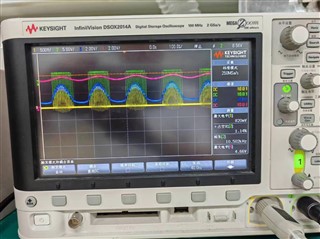
CH1:CS pin  CH2: OUT CH3:COMP CH4:pin1 for opto-coupler HPC1018. 

The primary inductor is 40uH.CTR of optocoupler is 130-260%. 
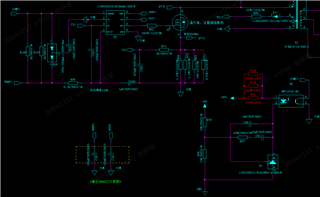
Can you help check what might cause the issue? This is new opportunity for us to gain business in new area. Looking forward to your reply!

  • Zoe,

    Here is how I approach flyback control loop compensation:

    1. From the schematic I do not see any startup resistor from the input voltage to VCC pin so it is not clear to me, how the startup is happening? VCC1 has 100nF (C34) but where is the bulk capacitance needed for VCC startup? There should be another capacitor in parallel with C34 (something like 1uF-4.7uF range). Make sure VCC is active, stable and above UVLO. For debugging the control loop, consider to supply VCC from DC lab power supply. Also, where is the output capacitor for the flyback bootstrap bias winding? You should show a capacitor connecte4d at R68 between VCC1 and COM.
    2. Temporarily, apply dominant pole to voltage error amp loop compensation. This can be done by temporarily setting C45=100nF and will force the voltage loop to be stable but the regulation and transient response will not be good. You can go back and adjust the voltage loop compensation after step 3 below
    3. Make sure the current sense is stable, amplitude is correct and has the optimal amount of RC filter applied
    4. Make sure the TL431 always has at least 1mA cathode current. Place a 1k resistor in parallel with opto-diode (U6, pins 1-2)
    5. Consider to change from TL341 (2.5V ref) to TLV431 (1.25V ref) which will be better suited for 5V regulation
    6. Model control loop: you can use the free TI Power Stage Designer which includes control loop modelling tool (loop calculator)
    7. Use the result from step 6 and go back to step 2 and apply the correct component values to the voltage amp compensator (C45, R97, C51, R75, R96)
    8. There is no slope compensation added - please add it
    9. The E2E thread title suggests UCC28C42 but the schematic shows U2 as UC3844?
    10. Measure the final compensated, closed loop response using a network analyzer and show that the loop is stable under all line/load conditions.

    Regards,

    Steve