Tool/software:
Please tell me the following.
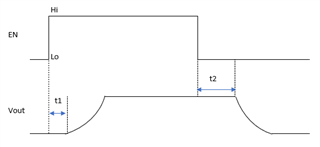
① What is the typ/min/max time that Vout starts to rise after the EN terminal voltage exceeds the Hi threshold (t1 in the diagram below)?
② What is the typ/min/max time that Vout starts to fall after the EN terminal voltage falls below the Lo threshold (t2 in the diagram below)
③ What is the typ/min/max value of the current that flows into the EN terminal?
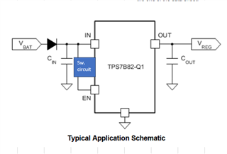
④ Please tell me the details of the circuit block inside the EN terminal.
⑤ Are there any resistors or diodes between the EN terminal and the GND terminal? If so, please tell me the resistance value.