This thread has been locked.

If you have a related question, please click the "Ask a related question" button in the top right corner. The newly created question will be automatically linked to this question.

UCC28782: Behavior when Vsw drops

Part Number: UCC28782

Tool/software:

Hello,

I would like to ask you about the behavior of UCC28782 when Vsw drops.
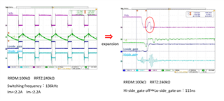
The attached figure shows the waveform when Vsw (Vds) drops.
When the low-side turns on, Vsw rises again. The part circled in red.
I would like to eliminate this part circled in red, is there a way to do this?
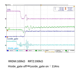
I also thought that I could eliminate the part circled in red by extending Tz, so I changed RRTZ from 240kΩ to 390kΩ.
However, Tz did not extend at all. Please let me know if there is a reason why Tz does not change.

Best regards,

  • Hi Kaji-San,

    Thank you for reaching out.

    1. it seems unusual Im+ and Im- equal to 2.2A. The resonant time is too long. I wonder we may need to check on the clamp capacitor. Try decreasing this value.

    2. If RDM is too high, the enforces high-side on-time will be too long. The tuner will be unable to compensate fully and too much negative current will be generated. This then increases the positive current to compensate for the additional power loss and it increases power loss even more.


    If RDM is too low, the high-side FET may turn off before the transformer has fully demagnetized, interrupting the active-clamp resonant current and causing high switching losses in the high-side FET and SR FET. And it will disrupt the tuner operation as it hunts back and forth to try to restore the optimal switching points.


    If RTZ is too high or too low, it will shift the turn-on point of the low-side FET to either side of the resonant valley of the drain waveform, leading to hard-switching instead of ZVS.

    So I think we need to tune this, reduce this with in conjunction with Cclamp value for best results.

    3. On the turn on of the high side pulse, can you try slowing the turn on of the low side FET, probably increase the gate resistance to see if this improves.

    Please let us know your observations.

    Regards,

    Harish 

  • Thank you for your reply.
    I adjusted the clamp capacitor and RRDM and got the waveform below.
    I think the waveform is optimized, but what do you think?

    However, efficiency has not improved compared to before the change.
    The reason we are considering this is to improve efficiency.
    Is the only way to improve efficiency to reduce Csw in order to reduce the effective value of the magnetizing current?

    I understand that reducing Csw reduces the negative primary side current when PWMH is turned off.
    However, I don't understand the principle behind the decrease in primary side current when PWML is turned off.
    Would it be possible for you to explain the principle behind this?

    Best regards,

  • Hi Kaji-San,

    Thank you for reaching out.

    I think the adjustment of RDM and clamp capacitor, the primary current looks much better now.

     1. The switch node capacitance has a lot to help reduce the RMS currents in the primary.

    2. You could also try tuning the full ZVS to partial ZVS to see if this is kind of helping. Although might not be the best for GaN case when compared to Si case.

    3. Cclamp could still be optimized further to have the resonance time higher than the PWM on time to help with the RMS currents as 1.8A still seems on the higher side.

    Overall, I think Cclamp, Csw, RTZ and Rdm still can be tuned further to optimize efficiency.

    Regards,

    harish

  • Thank you for your reply.
    Regarding point 3, is it correct that to lengthen the resonance time, the clamp capacitor should be increased?
    If the clamp capacitor is increased, the waveform reverts to the original, but if RRDM is increased the waveform does not change, and the device does not start up when RRDM is 300kΩ.
    The adjustment is difficult, so I would appreciate any advice you can give me.
    Best regards,

  • Hi Kaji-San,

    Thank you for reaching out.

    Yes, increasing the clamp capacitor will increase the resonant time. Ensure the negative Imag is less. 1.8A seems high.

    I think optimization should follow the following steps:

    1. So optimizing the switch node capacitance would help here.

    2. Use optimal value of C clamp and adjust as per PWMH ON time. Maybe resonant period is slightly higher than the PWMH on time.

    3. Optimze RDM and RTZ resistors.

    Regards,

    Harish