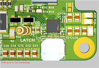
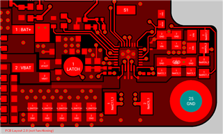
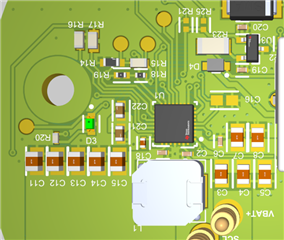
This thread has been locked.

If you have a related question, please click the "Ask a related question" button in the top right corner. The newly created question will be automatically linked to this question.

BQ25792: VSYS Falling Low after a few seconds

Part Number: BQ25792

Tool/software:

Hi, I am using a BQ25792, I am somehow damaging this IC however unsure what my be causing it because I haven't noticed a pattern yet. 

Once the IC is damaged, I can see on an Oscilloscope the output (VSYS) operates fine for about 10 seconds with a small load (100mA) however, slowly falls from its programmed regulated output voltage (~7.4V) across a few seconds after this point, until it reaches around 3V, ripples and then completely dies and there is no more output.  

After this, if I turn off VBAT wait a couple of seconds and turn it back on, the above occurs again instantly. If I wait a few minutes, then it'll operate fine for 10 seconds again and then die. It's happened on 3 IC's now... 

I have used this IC on a previous project and never faced this issue and have carried across the same schematic so I can only assume that I am damaging it either by my testing approach or something upstream. As it works for an entire day of testing until I must be doing something and breaking it. 

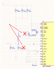
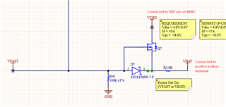
The only thing I can imagine is happening is I am supplying a voltage upstream on the VOUT rail when testing (no input on VBUS or VBAT), which is going into flowing back into IC and damaging it (shown by the arrows in my schematic below). Could the damage be caused by this and should I have a diode on VSYS to prevent this?

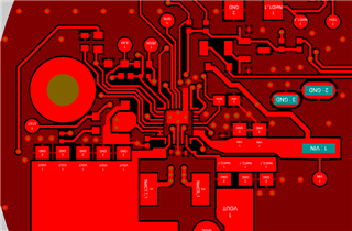
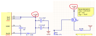
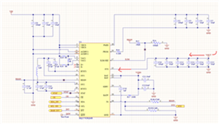
This is my schematic:


This is a close up of reference CH2 which is VSYS, once a load is applied after 10 seconds it drops to this

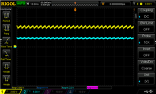
This is CH2, first outputting 7.4V from VSYS, with a load of 150mA for a few seconds, then it drops and crashes, then when the load is released it bounces back to a stable 7.4V output. When I replace the IC there is no longer this issue, so I know it’s not the load.


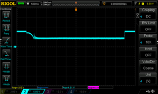
Thanks in advance for any assistance!

  • HI Michael,

    The charger wasn't designed for having an external voltage applied at SYS when in forward/charge mode. I have no data regarding if the IC can could be damaged.  Do you have have a data dump from the I2C register before the failure?  I recommend adding a diode.

    Regards,

    Jeff

  • I added the diode and that didn't resolve anything. I found the chip is not performing properly when just using purely VBAT input - nothing else connected (besides a small load on the output) so it wasn't my testing that damaged it.

    I don't have a data dump but I have concluded it is definitely something to do with the PCB layout. I have previously used this IC on a previous PCB design which never had any issues and I had followed the PCB layout recommendations accurately. By jumping the VSYS on that old PCB to VSYS (output) on my new PCB everything performs correctly and the BMIC doesn't drop out.

    I have also concluded the BMICs aren't actually damaged or broken, when removing them from my new PCB design and using them on the old they function as expected.

    Schematics are exactly the same between designs so I can only put it down to PCB layout. 

    The only questionable difference between the two PCB designs is the switching capacitors with the inductor on the new PCB design. To simplify assembly we attempted to place the two capacitors on the top side of the PCB (C10 and C9 in the images below). However in case this didn't work we also left the two capacitors on the underside of the PCB as the recommended layout suggests. We've tried populating it on both the top side, or on the bottom side but neither works. There is never four populated at the same time. (In the original design we only ever had them on the bottom)


    Attached below are photos of the old PCB layout and new PCB layout

    The new PCB (non functioning)


    The original PCB (functioning)

  • Actually, another reason might be because I have a P-Channel MOSFET between BAT pin on the BMIC and the positive battery terminal on the battery. This was added so we could connect a different BMIC (VFAST) to charge the battery at a faster rate than what this IC offers. The idea was, when there was a voltage present on VFAST it would disconnect the battery from the BQ25792.

    Although when testing VFAST isn't present perhaps the P-Channel is causing an issue with how the BMIC reads the battery...


  • I can confirm bypassing this MOSFET, the BMIC now works as expected. If possible it would be good to understand why the BMIC doesn't like the MOSFET between the BAT pin and the positive of the battery. Capacitance? Resistance?

  • HI Michael,

    The charger regulates the voltage at BATP pin not BAT.  I recommend back to back FETs so that the there is no current path through a body diode.

    Regards,

    Jeff

  • Sorry, I do have it wired to BATP as well (shown below). Thanks for your advice I will attempt back to back FETs as recommended and will click resolved should it work! Thanks again for your support