This thread has been locked.

If you have a related question, please click the "Ask a related question" button in the top right corner. The newly created question will be automatically linked to this question.

TLV759P: Vias under the thermal pad

Part Number: TLV759P

Tool/software:

Hello,

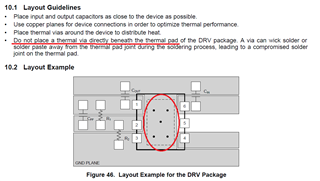
I have a question about the contents of page 22 of the TLV759 datasheet.
The guideline explains that vias should not be placed under the thermal pad.
However, in Figure 46, vias are placed under the thermal pad.
Is Figure 46 incorrect?

Best regards,

  • Hi Kaji@PAN,

    I'm surprised to see guidance in the datasheet that recommends against thermal via's inside the thermal pad.  This is one of the main methods of distributing the heat away from the device.  We of course recommend thermal via's in the thermal pad, but you should also check with the assembly house to confirm they can meet your solder joint requirements given a PCB design.  You don't want these thermal vias to have large inner diameter, for example.  I'll add this to our datasheet correction log and there should be an update here during our next revision of the datasheet.

    In our local design library, we use 2 thermal vias inside the thermal pad of this LDO with 20 mil outer diameter and 8 mil hole size.  More thermal vias is better if your assembly house can support it with your solder joint requirements.

    Thanks,

    Stephen