This thread has been locked.

If you have a related question, please click the "Ask a related question" button in the top right corner. The newly created question will be automatically linked to this question.

LMR14030-Q1: Schematic design suggestions

Part Number: LMR14030-Q1
Other Parts Discussed in Thread: LMR14030,

Tool/software:

Dears,

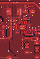
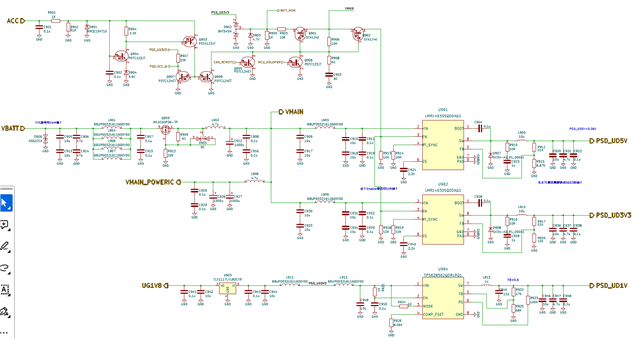
At present, during testing by end customers, it has been found that the VIN pin of LMR14030 is broken and short circuited to ground. The specific cause has not been found yet; The following diagram shows the design principle of our LMR14030-Q1. The entire power tree is fed with VBATT 9-16V and outputs 5.5V/3.3V/1.8V/1V respectively;

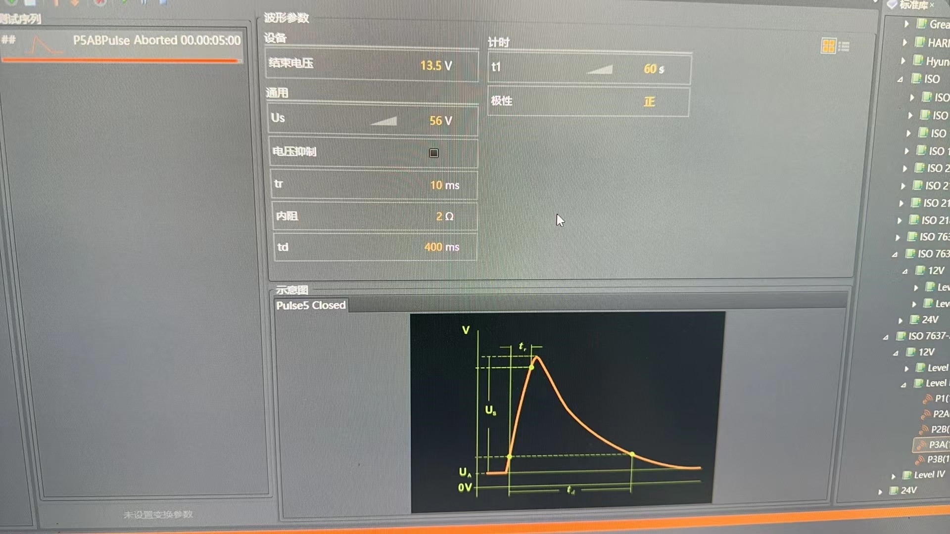
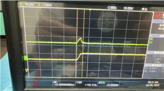
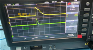
At present, we would like to inquire about the possible cause of damage to LMR14030-Q1. Is it a problem with the schematic diagram, and are there any suggestions for improvement? Currently, we have also found some significant fluctuations in the output voltage of the chip during the Pulse 5b test. Is this normal imagination?

Looking forward to your reply, thank you~

  • Hello,

    Based on your description it sounds like the device is experiencing electrical overstress. Are there any input transients you expect and if so what would the transient voltage be?

    With regard to your schematic my comments are listed below:

    • The input filter needs to have some damping capacitance. Please refer to this application note for guidance: https://www.ti.com/lit/an/snva489c/snva489c.pdf
    • The inductors are oversized for the application. Based on the RT resistor, it appears that the switching frequency is 2.2MHz. If that is the case, then I calculate 1uH for the 3.3V output and 1.5uH for the 5V output

    Are you able to provide the PCB layout?

    Best regards,

    Ridge

  • Hello, Ridge,

    Thanks for your response.


    1.Seeing your conclusion that was EOS damaged, according to the customer's description of this problem after the OTA upgrade, do you deduce what may be the cause?

    2. I did the ISO17650 pluse5A and 5B test for your called the  input transients. the detailed test background please see attached pic.

    3.For inductors,9-16V is normal condition, The worse case need to consider 36V for TVS capability.

    4.I atached the layout for your review.

    Thank you.

    BR Victor

  • Forgot the pluse 5B scppe,

  • Hello,

    Can you confirm the maximum voltage placed on the Vin pin during the pulse test? Based on your screenshot it looks like 56V is applied. If that is the case, then the test violates the absolute maximum input voltage of 44V and may be causing damage to the device.. For the oscilloscope image, what does each trace represent?

    Best regards,

    Ridge

  • Dear sir,

    The following scope maybe help to understand, Pluse 5A test, the max input is 65V,but there is a TVS in my power circiut which can clamped the input to 32.5V.

    The yellow: input voltage, green is output 3.3V.

    Thank you.

    Thank you.

    BR Victor

  • Hello,

    With the most recent screenshot it looks like the device was able to recover from the transient. In the case where damage occurs, it is important to have the damping, usually in the form of an electrolytic capacitor with sufficient ESR, to prevent ringing in the filter from violating the absolute maximum rating of the device. 

    On the layout, the input capacitors could be moved closer to the IC. Input capacitors, especially the HF bypass capacitance should be as close to the input pin of the device as possible. Right now, there is a significant distance between the capacitors and the Vin pin.

    Is the yellow trace directly on the input pin of the LMR14030 specifically? This issue seems to be a result of a stress placed on the input pin since the failure occurs only during this line transient test.

    Best regards,

    Ridge

  • Hello,

    Since we have not heard from you in a while I will be closing this thread. If you have more questions, you can re-open this thread by replying or create a new thread.

    Best regards,

    Ridge