This thread has been locked.

If you have a related question, please click the "Ask a related question" button in the top right corner. The newly created question will be automatically linked to this question.

TPS65987DDK: Questions regard device connectivity and Power up and

Part Number: TPS65987DDK

Tool/software:

Hello, 

I have two questions regard the device 

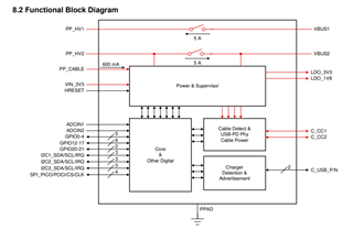
1. What are the D+/D- used for in the device? In the first page of datasheet they are connected while as far as I know, Power delivery messages are transferred only through the CC lines.

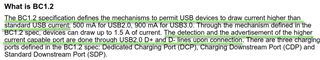
It then written that they support BC1.2 - what is it ? Why D+/D- shall be connected to that device ? 

2. How does the device turns up ? Shall it be connected through one of its I2C or SPI to an EEPROM where its SW is loaded from when power up ? Or shall it be connected through one of these interfaces to an MCU ? 

Thanks, 

Ohad

  • Hi Ohad, 

    Thank you for reaching out!

    1. Yes, PD messages are transferred through the CC lines. The D+/D- lines are used for BC1.2, which is a legacy charging specification (See the following application note for more information. Please note that BC1.2 is no longer supported on the TPS65987DK. Pins 50 and 53 can be utilized as GPIOs. 

    2. The TPS65987DDK can be configured by a host processor (MCU) via I2C or can load the configuration from flash memory (SPI) during the boot sequence. Please refer to the Technical Reference Manual for more information. 

    Please let me know if you have additional questions. 

    Best Regards, 

    Aya Khedr 

  • Hi Aya, 

    I'm not sure I understood. In the application note you sent it is written that BC1.2 specification is what enables USB devices to draw current higher than standard USB current and it is also written that it is done through USB2.0 D+ D- lines connection.  

    So does it mean that only by using BC1.2, which you claim is no longer supported by tps65987ddk, the device can transfer 5A??  

    If so than what is the tps65987ddk capability for current transferring without the BC1.2??  In datasheet it doesn't mention that only with BC1.2 5A/20v can be transferred. 

    BR, 

    Ohad

  • And another question - 

    What shall be the boot mode and what HW configuration for ADCIN1 (table 8.5) if I want the tps65987ddk to work only as a SOURCE for 15v/3A after starting up? Shall it wait to external 3v3 or VBUS and only then device shall continue start up?  

    Ohad

  • And another question: 

    Can PPHV1 and PPHV2 both be supplied by the same power supply of 15v when the tps65987ddk act as a source of 15v on the VBUS1/2 connected to the connector which will in turn deliver 15v/3A on the cable to the other end point?  

    Ohad

  • And another question regard the DRAIN1/2 pins: What shall they be connected to ? What do you mean by Thermal pad as big as possible as written in datasheet ?  What electrical connection shall be there ? GND ?  

    Ohad

  • Hi Ohad, 

    1- The BC1.2 specification was defined following the standard USB 2.0 and USB 3.0 specifications but prior to USB-Type-C and USB-PD specifications (see table below for the evolution of USB power from Primer on USB-C and USB-PD). In some applications, BC1.2 was required for backwards compatibility, but we are seeing very few cases that still require BC1.2 support, which is why it is no longer supported on the TPS65987DDK. 

    The TPS65987DDK is a PD controller following the USB-PD specification in which a maximum current of 5A is defined.

    2- In a source-only application, the dead-battery configurations are not really applicable. Therefore, ADCIN2 should be set to BP_NoResponse. 

    In the case when the configuration is not available during boot process, a device configuration from the table below should be set according to your application. 

    3-You would only need to utilize one power path switch for source-only application. The other power path can be grounded, if unused. VBUS1 and VBUS2 should be tied together. 

    4- The Drain pins should be connected to each other and there should be a pad on the layout for heat dissipation. Please see section 11.6 Thermal Dissipation for FET Drain Pads in the datasheet for more information. 

    Please open new threads for separate questions for better trackability. 

    Best Regards, 

    Aya Khedr 

  • Hi Aya, 

    Regard question 1 - No configuration in the table you sent me relates to "Source only". What is the boot for that case? 

    Regard question 2 - ADCIN1 is for the boot configuration. ADVIN2 is for I2C address. So did you mean to config BP_NoResponse on ADCIN1 ? 

    Regard question 3 - Which PPHV to use for Source only? 1 or 2 or both ? 

    Regard question 4 - So Drain Pin shall be connected only to thermal PAD and that's it ? 

    Ohad

  • Hi Aya, 

    Is there any answer for my questions? 

    BR,

    Ohad

  • Hi Ohad, 

    Regard question 1 - No configuration in the table you sent me relates to "Source only". What is the boot for that case? 

    Regard question 2 - ADCIN1 is for the boot configuration. ADVIN2 is for I2C address. So did you mean to config BP_NoResponse on ADCIN1 ? 

    My apologies, I meant to say ADCIN1 should be set to "BP_NoResponse" for dead battery mode. In terms of the device configuration, if loading the patch bundle via EC, the device configuration should be set to "Infinite Wait". If loading the patch bundle via SPI flash, then the configuration should be set to "Safe"

    Regard question 3 - Which PPHV to use for Source only? 1 or 2 or both ? 

    Typically, PPHV1 is configured as a sink path and PPHV2 is configured as a source path. These can be configured in Global System Configuration (Reg 0x27) in the GUI. 

    Regard question 4 - So Drain Pin shall be connected only to thermal PAD and that's it ? 

    Yes, the drain pins should be connected to their respective Drain pads underneath the IC to help with thermal dissipation. 

    Best Regards, 

    Aya Khedr

  • Hi Aya, 

    There is a kind of a conflict between datasheet to EVM doc in regard to BP_NoResponse configuration.

    In datasheet it is written that the value configured by the resistors divider shall be: 

    Which means the value for BP_NoResponse shall be ~0.09 that sits in the middle between 0 to 0.18. 

    While in EVM scheme it looks the value from the resistors divider is 0 (PD of 100k) which is not the centered value as mentioned to be in sata-sheet. 

    Why is that conflict: 

    Then what is the right way to do? 

    Ohad

  • Hi Ohad, 

    It is best to follow the datasheet's recommendation. The implementation on the EVM was slightly limited due to the use of the ADCINx switch. 

    Best Regards, 

    Aya Khedr