Tool/software:
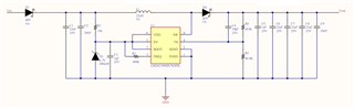
We are using the LM2621 to boost a "9V" battery to 12V to power an MCU and a electro-mechanical lock. The MCU controls a high side switch to power the electro-mechanical lock. A flyback diode protects the high side switch (and boost) from the electro-mechanical lock as it may be a solenoid based locking mechanism. Additionally, a 3A fuse is between the boost circuit and the mcu/lock load.
This circuit works fine for most locks but we recently tested against a lock that consumes 1.2A max and 200mA at typical idle. After powering/controlling the lock the LM2621 no longer boosts the input voltage to 12V (input voltage is passed through with the expected diode drop). This has been reproduced on 2 separate devices.
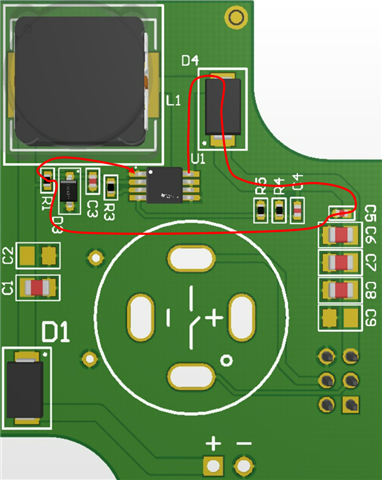
A visual inspection of the LM2621 in one of the failed devices shows a burn mark above/near pin 7 and pin 8:

From the picture, is it possible to determine what failed on the LM2621? What part of the chip is under the burn location?
The 3A fuse protecting the load is not getting tripped.
Pin 7 (boot) (in addition to EN and VDD) are limited by a 4.7V Zener and are powered from the input voltage so I don't think pin 7 was subjected to over-voltage.
Pin 8 (sw) - There is no evidence that the LM261 output was shorted to ground. The LM2621's internal current limit should have protected the chip if an in-rush current current occurred. Additionally, I would have expected the thermal protection to kick in case of too much current flow through the internal mosfet.
Any thoughts on what is going wrong?