This thread has been locked.

If you have a related question, please click the "Ask a related question" button in the top right corner. The newly created question will be automatically linked to this question.

UCC28740: UCC28740 not switching and FB pin

Part Number: UCC28740
Other Parts Discussed in Thread: PMP9638, LM341, TL431

Tool/software:

Hi, 

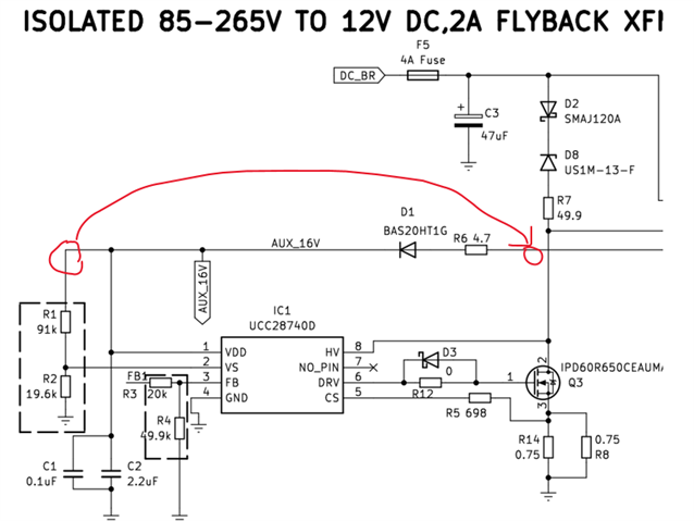
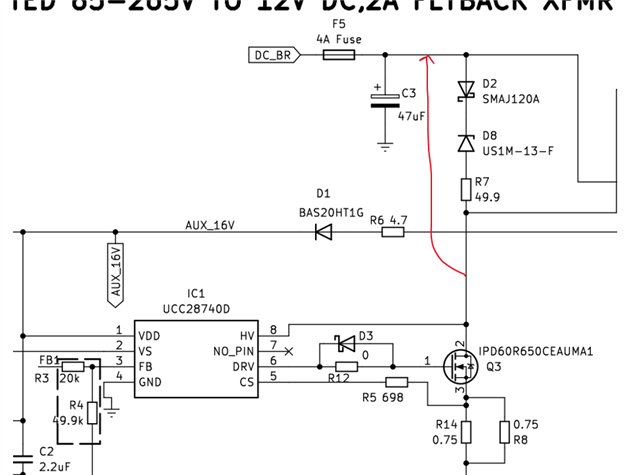
I need help with the UCC28740 design based on the PMP9638 reference design. 

1) Why is it not switching? The schematic is attached. My Auxiliary winding is intended for 20V but its reading 15V. 

VS pin = 2.45V

VDD pin =14.20V

HV pin =  332V

CS pin - no reading 

DRV - No reading 

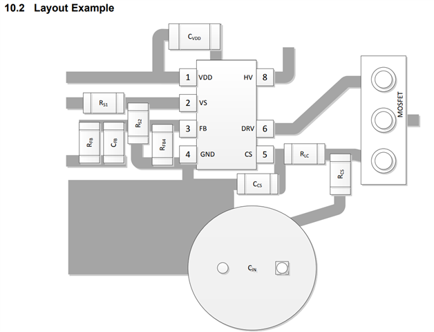
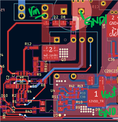
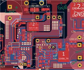
What could be the problem? I have also attached the  PCB layout. 

I have test the MOSFET and Diode, they all work fine. 

2) Is there a way of checking whether the IC is damaged?  (I doubt so)

3) Based on the PMP9638 reference design, the FB pin is receiving more than 7V which is the absolute maximum rating (UCC28740 datasheet ) if 20K and 49.9K acts as a voltage divider. How does it work?

 Schematic_PMP9638.pdfPMP9638.pdf

Kind regards,

Bright

  • Hi, 

    Just to mention, The auxillary voltage of the transformer is dropping from 20V to 14V. I have changed the transformer to 750314727 but it is still dropping to 14V. What might be the problem?

    Kind regards,

    Bright

  • Hi Bright,

    I will be back to you Monday morning

    Thank you

  • Okay. Also, is the R11 from the reference design is 95.3k but when I calculated it, it give 9.53k. Vref of LM341 is 2.5V, R_upper 9.53k and R_lower 2.49k, gives approx 12V. The 95.3k will give 98V. 

    Vout = Vref x (1+R_upper/R_lower) . 

    Please comment. This may explain why my auxiliary is giving 14V instead of the 20V. It appears as though the IC is switch, if it was not, no pulsating DC will be seen at the auxiliary winding output. 

    Kind regards,

    Bright

  • HI Manuel,

    I am still waiting for your response. 

    Kind regards,

    Bright

  • Okay. Also, is the R11 from the reference design is 95.3k but when I calculated it, it give 9.53k. Vref of LM341 is 2.5V, R_upper 9.53k and R_lower 2.49k, gives approx 12V. The 95.3k will give 98V. 

    Vout = Vref x (1+R_upper/R_lower) . 

    Please comment. This may explain why my auxiliary is giving 14V instead of the 20V. It appears as though the IC is switch, if it was not, no pulsating DC will be seen at the auxiliary winding output. 

    Correction: I changed the resistor to R_upper to 10k and R_lower to 6.39k with a potentiometer but no Vout reading. And the N MOSFET is not showing any signal, but still the auxiliary winding is showing 14Vout instead of 20V.

    I have used two different transformers of the same type but different manufacturers and it is still the same issue. 

    What could be the issue?

    Kind regards,

    Bright

  • Bright,

    There is an error on the voltage divider resistor values of the Reference design schematic PMP9638. Top resistor should be 9.53Kohm. If 95.3koms was used, UCC28740 will trigger OVP (over voltage protection) at the VS pin and it will shutdown and stop switching. Please, change resistor to 9.53Kohms and check again.

    Thank you

  • Hi, 

    you have not provided any sufficient response regarding the  question raised, and not even sure that you read through my comment. 

    I mentioned already that I have changed the  voltage resistor values of the reference design schematic PMP9638 to top resistor 10k and lower 6.39k, Vref of the TL431 is 2.5V, Vout is approx 12V. 

    1) There is no output voltage

    2) The N channel Mosfet gate is not showing any reading when measured with an oscilloscope 

    3) The auxillary voltage is reading 14V instead of 20V. Could it mean that it is switching or the IC is turning off and ON, because there is no gate signal seen with an oscilloscope. But the MOSFET needs to switch in order to provide a pulsating DC. 

    Finally, I am not satisfied with your response, it shows lack of technical support.  kindly refer me to another person that can provide technical support if you are unable to do so. 

    Kind regards,

    Bright

  • Also, there is no mention of the PCB layout, which I have attached earlier,  suggesting that you did not attempt to review it. 

  • Correction: Top resistor 24.3k and lower resistor 6.39k

  • Bright,

    Apologies for the incomplete response. Please, see below my notes and layout review. Let me know if you have any questions,

    1. I noticed that R1 and R2 resistors are connected after diode D1, btu they should be connected at the AUX net. If those resistors are connected after D1, VS will be reading positive DC Voltage (VDD-GND) and the controller will never pull down the I_VS_RUN current (225uA typical value) from VS pin to start the converter after the first three PWM pulses. VS should read negative voltage coming from AUX voltage. Please, correct that.

    2. Layout:

    -VDD pin:
    Good: C1 and C2 are connected next to VDD pin.
    To improve: The return connection of C1 and C2 should be as short as possible to GND pin for better decoupling. Place a GND trace underneath IC1 to connect directly to GND pin rather than connect it to the ground plane. You move the trace of the diode D1 to VDD pin in the bottom layer.

    -VS pin: 
    Good: Short trace between the voltage divider net (between R1 and R2).
    To improve: The return connection to GND from R2 should be as short as possible to avoid any EMI coupling from noisy traces. Place a GND trace underneath resistor R3 and R4 to connect directly to GND pin rather than connect it to the ground plane. Please, correct the resistor divider connections to VAUX.

    -FB pin:
    Good: the secondary side of the optocoupler is close to FB pin to minimize the loop and avoid ant EMI coupling.
    To improve: R4 return connection should be connected directly to GND pin rather than connected to the ground plane. I recommend swapping R3 and R4 resistor positions so R4 us next to (FB-GND) pins.

    -HV pin:
    Not sure why HV pin is connected to the clamp resistor in the reference design. HV is a high voltage start-up pin that can handle up to 700V, so you can connect HV pin directly to DC input voltage net.
    Good: The HV trace is away from the signal low voltage traces.
    To improve: Keep the HV trace away from DRV pin. DRV pin is very noisy due to the high dv/dt. If possible make the trace perpendicular to DRV trace specially the area close to the HV pin. 


    -DRV pin: This trace is very noisy and should be away from other signals. Ideally, it should be perpendicular to HV and CS trace to avoid any EMI coupling. No need for R12 and D3. R12 seems to be a 0ohm resistor, so it should be ok. You can get rid of D3.

    -CS pin: make this trace perpendicular to DRV trace wen connecting to R5. The return connection of the current sense resistors R8 and R14 should be as close as possible to input bulk capacitance C3 to close the loop and avoid parasitic components coming from PCB. Consider moving C3 closer to the controller or use vias to connect the return of resistors directly to negative of C3 rather than connecting to the power ground plane. Please, see below a good example of a layout from the Datasheet.


  • Hi Manuel,

    Thank you very much for the review and response. This is exactly what I was looking for. You've done wellSmiley

    I have attached the update PCB layout based on your recommendation, perhaps you could comment the new PCB layout.

    Kind regards,

    Bright

  • Also, what is the advantage of not connecting those traces to ground plane, as you have recommended to connect them directly to GND pin. Thank you

  • Bright,

    Good job. Your layout looks better now. The reason why we should connect signal trances and decoupling capacitor connections directly to the signal pins is because we want to avoid any noise coupling to the signal current traveling through the traces. Ground copper planes, even though they we are good for providing low impedance connections and good thermal dissipation, they are noisy and are susceptible to catch any EMI noise in the environment. Signal pins like VS and FB need to sense Vout (through aux winding) and feedback current very accurately in order to provide accurate response to the controller.

    Let me know if the VS resistor divider connection fixed the issue.

    Thank you