A related question is a question created from another question. When the related question is created, it will be automatically linked to the original question.
If you have a related question, please click the "Ask a related question" button in the top right corner. The newly created question will be automatically linked to this question.
[FAQ] UCC21750-Q1: Isolated Gate Drivers Power up Sequence
In complex end applications, multiple power rails exist. It is critical to define appropriate power-up and power-down sequence of different power rails, in specific order to avoid violating device specifications or other potential issues.
Advanced semiconductor devices like isolated gate driver (UCC217xx), have multiple power supply pins (VCC1 and VCC2 (VDD) and VEE), primary side IO pins (IN+, IN-, RDY, FLT, /EN, APWM) and secondary side IO Pins (AIN, OC/DESAT, CLMPI/E).
The isolated gate driver has 2 separate reference grounds and respective supply pins: low voltage (LV) side power supply pin (VCC1) and high voltage (HV) side power supply pins (VCC2 /VDD and VEE). The power supply pins are supplied with onboard bias supplies. These LV and HV power supply pins are independent of each other and hence it can be powered up in any order. Typically, LV side is powered up first before powering HV side.
The isolated gate driver IO pins, especially the LV side IOs are typically connected to microcontroller GPIO lines. The isolated gate driver power supplies can be powered with different power rail from microcontroller. If the microcontroller is powered up first, then the GPIO lines can potentially be in high state during power up and it can drive the gate driver IO pins high before the gate driver supply pins are powered up.
This will cause the gate driver to power up through the IO pins which may damage the device permanently. Also, If the IO pins have push-pull inverter, then powering IO lines > supply voltage, can potentially create latch up condition. So, it is important to power up the power supply pins first before powering the IO lines. It can be achieved by having microcontroller and gate driver powering up at same time by using same power rail. Similarly, in the HV side, IO pins, especially AIN shouldn’t be powered before the VDD/VEE pins powered up.
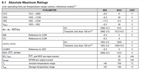
In the below Abs max table LV side IO pins max value is VCC, so when powering IO pins first it violates the device’s absolute max rating and shouldn’t be violated for safe operations.
In Summary:
1. Low voltage and High voltage sides can be powered independently. But general practice is to first power up the Low voltage side
2. Ensure that the IO pins of the gate driver is powered only after powering the device. Low voltage side has to be powered before powering its IO pins, similarly High voltage side has to be powered first before powering its IO pins.