


Hi,
I purchased the BQ20Z65EVM board and am currently studying the layout. I've noticed that the traces for the intermediate cell voltages (P1, P2, P3 - in boxes below) are significantly smaller than the traces for the extreme voltages (N1, P4).
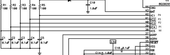
During the cell balancing process - cells with higher voltages will have the charging current bypassed through these traces (Is this correct?). Under this logic should all of the 'cell balancing' traces on BQ20Z65EVM have traces that are wide enough to handle the max charge current? If so, what is the maximum charge current that can be used on this board?
The traces for P1, P2 and P3 on the BQ20Z65EVM appear to be about 5 thou. As a result they would not be able to bypass the 2amp current my charger provides (constant current phase). I'm missing something?
