Other Parts Discussed in Thread: LM5123-Q1
Tool/software:
We are currently testing a boost converter design with the LM5123-Q1 boost controller and are having questions regarding the bypass mode of the controller.
We’re having trouble understanding the intended operation.
Our design is intended for 12V input to a 25.4V output boost converter with app. 130W power for automotive applications. We would also like to have the wide operating range as a feature in case this converter is connected to a 24V supply system.
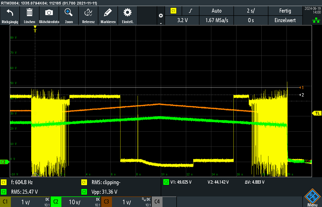
When testing the design on a 24V system we found some behaviour of the controller we don’t quite understand. Our understanding of the LM5123 is, it enters bypass mode when Vsupply rises above Vovth (108%). During bypass operation the charge pump is always enabled, so the high-side mosfet has 100% turn on time. (Pin 14 CP is connected to Vcc to be >2.0V).
What we found is, that sometimes the controller goes into sleep mode and the charge pump is no longer active even when the input voltage is above 28V.
When changing the supply voltage in the area of 27V to 30V, sometimes the charge pump is still active, providing Vsupply + app. 5V on the HO Pin, but sometimes when doing voltage changes (for example going from 27V to 28V) the HO and HB voltages drop to Vsupply, which in turn obviously turns off the high side mosfet and all current is flowing across the body diode. The test was done with 2-3A output current.
Maybe there is some input you can give us which explains this behaviour. From our perspective it should be possible to maintain 100% turn on time during bypass operation with the LM5123.
Thanks in advance