A related question is a question created from another question. When the related question is created, it will be automatically linked to the original question.
If you have a related question, please click the "Ask a related question" button in the top right corner. The newly created question will be automatically linked to this question.
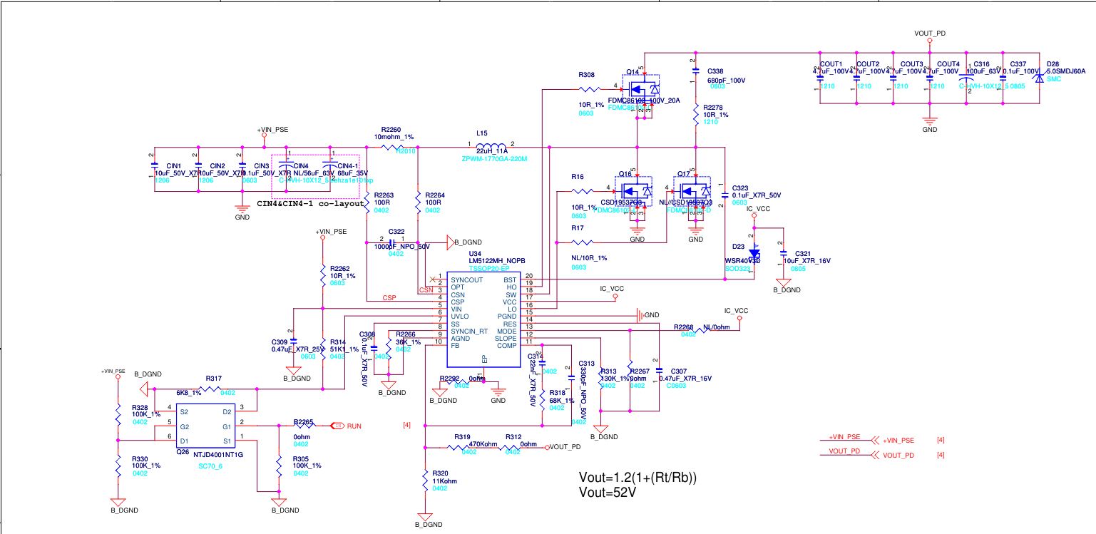
Regarding schematic: Inductor selection, capacitance, sense resistance and feedback loop all look good to me. Only one point of improvement is the VCC cap connection C321, which is currently connected to analog GND. As this cap supports the gate driver voltage, there is some current flow at this cap, so it is recommended to connected it to power GND.
Regarding layout: The switch node spreads across a large area and goes from top layer to bottom layer, which can can with risk of non-optimal EMI performance, but there is a large amount of vias to connect the planes, which improves the situation.
As pointed out on the schematic, VCC cap is placed at digital GND and not power GND. VCC should be connected close to the PGND pin and it should be kept in mind that the gate driver current patch is from LO to MOSFET gate, and back from MOSFET source to PGND. (Or from HO to MOSFET to SW pin) This loop should be kept small to avoid noise.
The digital GND is spread around several small islands within the boards. I would recommend to make this one small compact island if possible.
If possible, place output ceramic caps closer to the high side FET to minimize output voltage ripple.