


Other Parts Discussed in Thread: TPS40210
Tool/software:
Chasing down the cause of poor load regulation on a 28-40V input, 150V/400mA out boost converter designed for CCM operation. It will idle at the correct 150V and with load rapidly drop to 142-144V, depending on input voltage. No real problems with stability discovered so far, efficiency is right where it should be, seeing 94% at full load and happy with that. The TPS40210 Quickstart spreadsheet has been used to design for 350kHz switching.
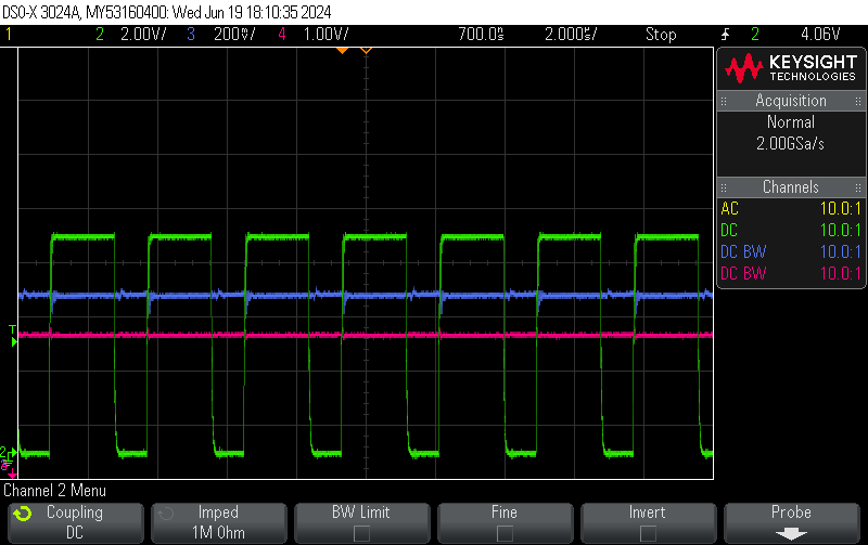
At 40V in and 40mA load, everything looks fine. CH2 is GDRV, CH3 is FB, CH4 is COMP
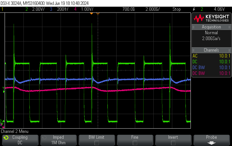
At 50mA ringing appears on GDRV and there is an FB anomaly the following on-period. Output voltage is dropping slightly.
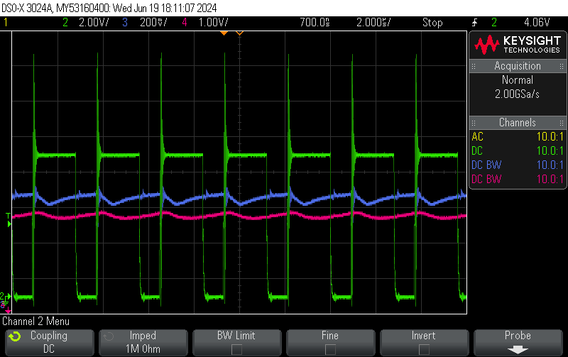
At 90mA output the situation has stabilized. All cycles have the GDRV ringing and all cycles have the FB anomaly.
It looks to me like there is causality between the GDRV ringing and the FB anomaly. From the device block diagram it appears that the only two possible sources of the FB anomaly is SS and VRef. SS is stable as a rock, leaving Vref as the culprit. Any ideas for a cure? Is this merely a layout issue or is there something more sinister going on?

