This thread has been locked.

If you have a related question, please click the "Ask a related question" button in the top right corner. The newly created question will be automatically linked to this question.

LM22679: schematic

Part Number: LM22679

Tool/software:

Hi Expert, 

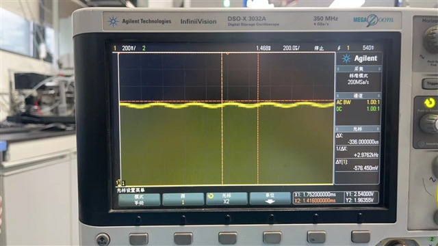
We are currently using the LM22679-ADJ chip, and when the ground of the bypass diode and the output power ground are connected together, there will be a ripple of 1.8kHZ on the output power supply, and a 1.8kHZ noise will also be superimposed on the SW pin square wave. could you help to give some advice? thanks. 

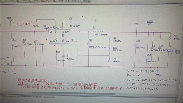
here is the schematic:

BR

Chi

  • Hi Chi,

    Please also provide the PCB layout.

    For the schematic:

    • The inductor looks oversized. For 12Vout, 6.8uH is recommended. Even though the customer plans to operate at a light load, the inductor should be sized for the full load capability of the device, 5A. Also make sure that the saturation current rating is greater than the HS current limit of the device.

    Can you clarify what you mean by connecting the diode GND to the output GND? The ground connections should all be on the same GND plane of the PCB.

    Best regards,

    Ridge

  • Hi Ridge, 

    thanks for your advice, here is the PCB layout, 

    Can you clarify what you mean by connecting the diode GND to the output GND? The ground connections should all be on the same GND plane of the PCB.

    it is means using the same ground here.

    BR

    Chi

  • Hi Chi,

    Can you expand on the SW node waveform? We would to see the high side of the SW waveform.

    Where is the scope probe grounded?

    What is the ESR of the output capacitors?

    Please provide Vin and Vout waveforms as well.

    Best regards,

    Ridge

  • Hello,

    Since we have not head back in a while, I will be closing this thread. If you have more questions, you can open a new thread or re-open this one by replying. 

    Best regards,

    Ridge