This thread has been locked.

If you have a related question, please click the "Ask a related question" button in the top right corner. The newly created question will be automatically linked to this question.

UC3846: Control Issues with UC3846 in Push-Pull Converter at Duty Cycles Above 0.5

Part Number: UC3846
Other Parts Discussed in Thread: TL431

Tool/software:

Hello,

I am using the UC3846DW controller to manage a push-pull converter. The input of the push-pull varies between 18 and 30V, and the output is regulated to 100V. With the knowledge of the input and output voltages and the formula that relates them to the duty cycle, it can be determined that the push-pull operates with a duty cycle between 0.33 and 0.55.

Vout=Vin⋅Duty⋅Transformer RatioV_{out} = V_{in} \cdot \text{Duty} \cdot \text{Transformer Ratio}Vout=VinDutyTransformer Ratio Transformer Ratio=10\text{Transformer Ratio} = 10Transformer Ratio=10

However, in the tests conducted, I have observed that with duty cycles above 0.5, the control starts to fail. Upon analyzing the documentation, I found an application note titled "MODELLING, ANALYSIS AND COMPENSATION OF THE CURRENT-MODE CONVERTER" which indicates that when controlling in current mode with duty cycles above 0.5, a compensator needs to be added.

Do you think it is necessary to add this compensator? And if it is necessary, how could I do it?

Thank you for your assistance!

https://www.ti.com/lit/an/slua101/slua101.pdf?ts=1718801260467&ref_url=https%253A%252F%252Fwww.ti.com%252Fproduct%252Fes-mx%252FUC3846%253Fbm-verify%253DAAQAAAAJ_____7iBEvfcvVARWpHWrS2pbEFZYHXV26-Dp5_IID9Amc5vj3Ta_QOr4GWiPst7MNaNh74Wu7I1JMQNt3u1yERH1VtAyN9-W8qzftu-VRQ6bLzrxrLDPo9Z5sZaelH-r8T3epwN8Hu-yaVOZwq_uO9nOnOnu43JYTVG5cy4KkWtbgVQhUN6mFbihfgUUXf__Al6xmxPDIfy7T2Eq5t98EXySbIpQugGpQnMLLbqnj2bt4hb-Fn26OKMuVbBZADIP23_4avhWVSnH0ePtmKsSndq79cwhnd2IQjF8bO9dBTYLnGjmAFnm3xVxkDv

  • Double ended controllers such as UC3846 are limited to 50% duty per output. when considering delays, temp and tolerance, the practical max duty limit is probably closer to something like 45%-47%.

    The added compensation you are referring to called slope compensation and is needed for peak current mode control operating at greater than 50% duty cycle. The push-pull/half-bridge topology cannot operate above 50% duty cycle and the magnetizing current is naturally balanced by the double ended symmetrical nature of the switching waveform.

    Regards,

    Steve 

  • Hello everyone,

    I agree with what you said, but I asked the wrong question before. Let me ask it again in more detail:

    Current design.

    The current design have four diodes in the secondary (see the next figure) and this are the parameters of that push pull:

    • Input voltage: 20 – 30V
    • Transformer ratio: 6
    • Output voltage: 100 V
    • Duty cycle: 0.14 – 0.21

    Modification in the secondary.

    To reduce the size of the heatsink, I made a change in the secondary, removing two diodes (see the next figure). This adjustment shifts the MOSFETs' operating point while maintaining the same output voltage. With this modification, the duty cycle varies between 0.28 and 0.42 to obtain 100 V at the output with input voltages between 20 and 30 V and a transformer ratio of 6.

    Problem.

    I've noticed that with this modification, the control has become unstable, and there is an imbalance in the semiconductor gates (see the next figure). This only occurs when the control is active; in open-loop operation, the push-pull works properly without any issues.

    Question.

    Could this instability be due to the push-pull now having to operate at higher duty cycles? Could adding a compensator be the solution?

    I hope you can help me with this issue.

    Thank you in advance for any assistance or suggestions.

    Best regards,

    Mikel

  • If you add a center tap to the secondary to use 2 output rectifiers instead of 4, the duty cycle will increase by 2x. If you reduce the center tap turns by 2, then you will see the same duty cycle you had previously.

    If the controller is not stable at the higher duty cycle, this is likely because the control loop compensation is not adequate at the new operating conditions or the optocoupler is not not biased correctly. Check CS, COMP, FB and opto/TL431 (if used). Measure the control loop and be sure you have sufficient phase margin? Make adjustments to the control loop compensation as needed.

    Steve

  • Hi Steven,

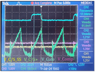
    Measuring the parameters you mentioned, I have another question. In the following image, the signals you mentioned in the previous message are shown. In this image, the control is working correctly and we have the desired voltage at the output.

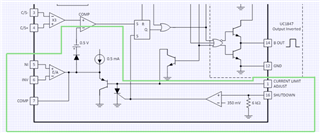
    However, analyzing this waveform, I have noticed something. The peak voltage of V_C/S+ is approximately 200mV, and since the chip has an internal gain of three (as shown in the next image), the voltage at the comparator is 600mV. The current protection (V_C/S_SS) is set to 1.25V, and the voltage at the COMP pin is 1.7V.

    With these limits, why is it regulated well at 100V? Shouldn't the current protection activate earlier?

    Thank you for your assistance.

    Best regards,

    Mikel

  • I believe we resolved the original post. If more help is needed please post a new thread topic.

    Steve