Tool/software:
Hello,
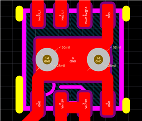
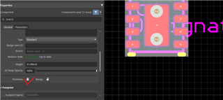
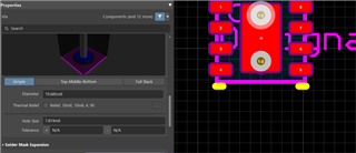
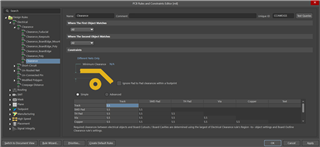
I am trying to solve this issue within the DRC for Altium PCB Editor (issue is this error: Routing Via Style: Via (1584.646mil,2601.541mil) from Top Layer to Bottom Layer Actual Size : 19.685mil Actual Hole Size : 7.874mil). Is there a way to edit the size of the ground via? I have attached an image below for a view of the via. I believe it's an issue with the wire being too large for the via. I was not able to find this option in the IC properties, and since I am using a TI template for the layer stack, it would not let me edit the wire size.