Other Parts Discussed in Thread: UCC27524, ISO7240CF, UCC27714, UCC28950, UCC27714EVM-551
Tool/software:
I’m working on bringing up a PSFB power supply design based on the UCC28951. Final goal is to reach 48VDC @ 90A with input voltage 60VDC to 200VDC. The webench design report I have based my design on is attached along with my final schematics.
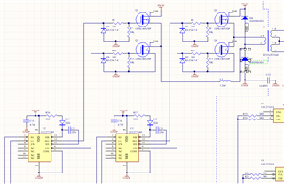
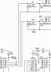
WBDesign3 (2).pdfJQ101A-SchDoc.pdfJQ102A+Mods-SchDoc.pdf
So far, I’ve been just trying to get it running at 60VDC in and very light output loads from 0 to 4amps. The output voltage is correct at 48VDC but I’m concerned about some high voltage ringing on the secondary and quite low efficiency
.
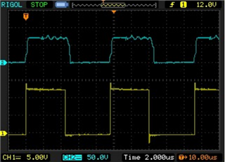
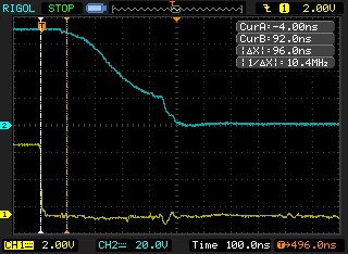
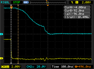
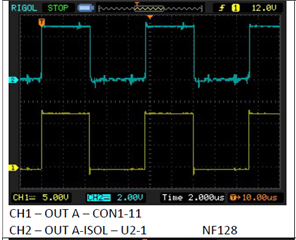
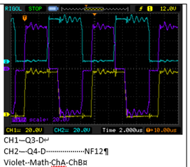
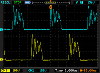
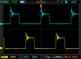
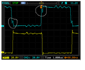
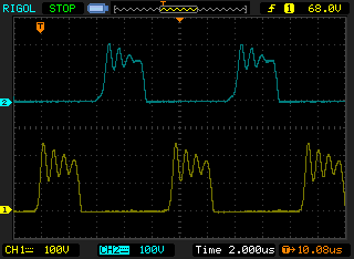
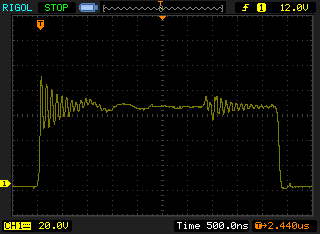
The above scope shot is:
CH1 = Q6-D-S, CH2 Q7-D-S (Output Fets).
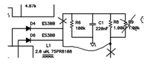
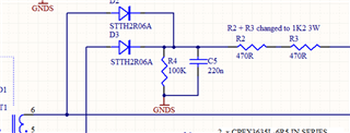
The RCD snubber circuit is fitted, R2-R3 resistor replaced with 3W 1K2 resistor gets smoky hot after about 30sec.
Vin is 60V @ 1.2A (72W) Vout is 47.7V into 47R load (48.4W) efficiency 67%.
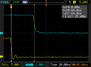
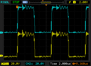
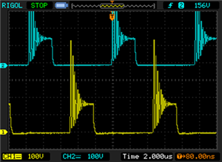
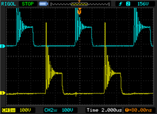
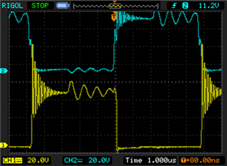
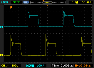
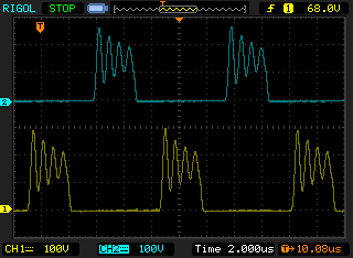
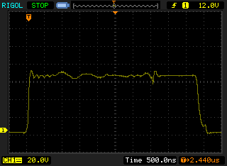
So, I tried removing the RCD snubber and this is what I got:
Very high ringing voltage spikes. Vin is 60V @ 1.493A (89.6W) Vout 47.7V 47R load (48.4W) efficiency 54%.
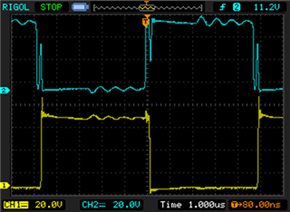
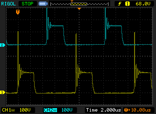
So, I decided to try adding an RC snubber directly across the Q6 Q7 fets D-S. After much trial and error I came up with 5nF 0R39 RC.
Vin is 60V @ 1.2 (72W) Vout 47.7V 47R load (48.4W) efficiency 67%.
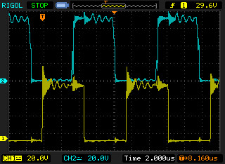
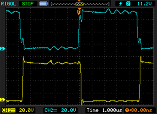
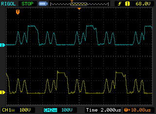
And ringing increases with increased load as shown below.
Vin is 60V @ 2.4 (144W) Vout 47.7V 23.5 load (96.8W) efficiency 67%.
With both the RC snubber and the RCD snubbers fitted there is some more improvement in the ringing but efficiency goes down and the RCD snubber resistor heats up.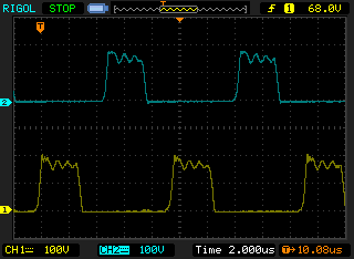
Vin 60V @ 1.424A (85.4W) Vout 47.7V 47R load (48.4W) efficiency 57%.
All of the above is with Q6, Q7 disabled with the gate tied to ground with 10R resistor, because at low power levels the synchronous fets are not operating and just the internal diodes are used.
As a test I tried replacing Q6, Q7 with diodes S3D50065D1.
Iin 985mA @ 60V (59.1W) Vout 47.7V 47R load (48.4W) efficiency 82%. So, efficiency is looking a lot better but I am not sure about ringing either side of main pulses.
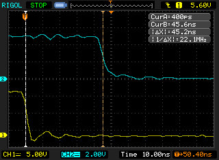
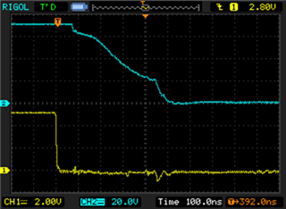
I also had ringing on the primary FETs Q3 and Q4.
Above is ringing on Q3. I improved with 5nF 6R RC snubber across D-S as shown below.
And this was ringing on Q4

Improved with 5nF 6R RC snubber as shown below.

So, my questions are:
Why all this ringing? I don’t see RC snubbers being used on other UCC28951 circuits and evaluation boards.
Why is the RCD snubber as shown on WeBench design and evaluation boards consuming so much power? Is this normal at such low output powers causing very poor efficiencies at light loads?
What should I be doing to progress this design to the higher output powers I need, not just 1-4 amps but up to around 90A. I’m worried everything will just get worse as the powers increased. I think the ringing is already causing interference with the control card and I had a lot of the UCC27524 gate drivers destroyed when it was connected to Q6 & Q7.
Any advice much appreciated. I have spent a lot of time just getting to where I am now and seems a long way to go to get it to full power.