This thread has been locked.

If you have a related question, please click the "Ask a related question" button in the top right corner. The newly created question will be automatically linked to this question.

UCC27714: MOS driver

Part Number: UCC27714

Tool/software:

Hello,

When I use the UCC27714 to drive the H-bridge,  shoot-through often appears。

I want to know if there is any irrationality in the circuit design。

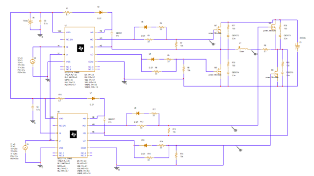
fig1: H Brigde,Current sensor, and my load is 10mH inductance between XL1/XL2
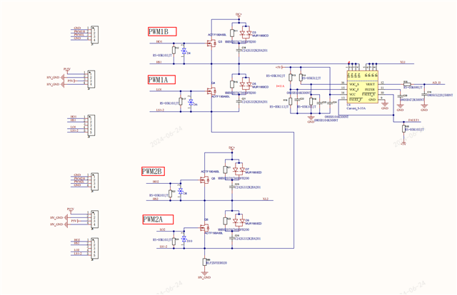
fig2:  drive circuit

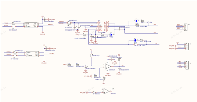
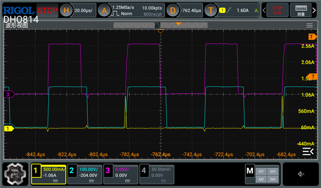
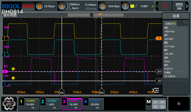
fig3: My test waveform,deadtime==4us.

CH1,CH2: PWM1A ,PWM2A

CH3,CH4:PWM2A ,PWM2B

 ;

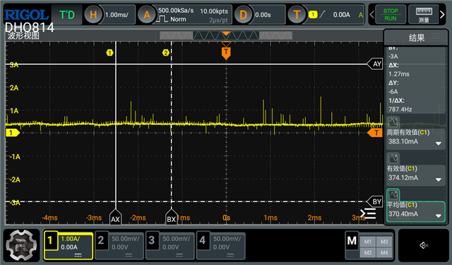
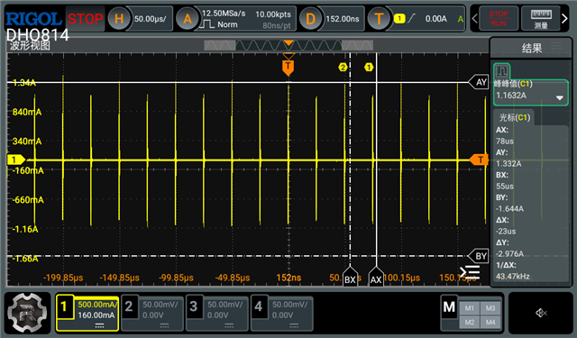
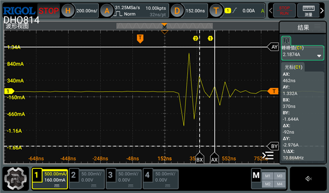
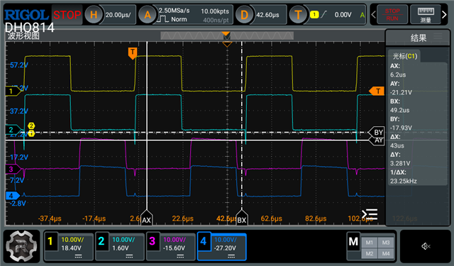
fig4: This is the current waveform when I run it correctly,Another question is what adjustments I need to make to reduce these current pulses

  • Hey,

    Thank you for reaching out to TI with your question regarding the UCC27714. I have a couple questions to better understand your setup and issue.

    1. Are you turning on both FETs in each half-bridge at once? It appears that way in the first waveform you shared with PWM2A and PWM2B being high at the same time. If this is the case, you will see shoot through as the DC bus will be connected directly to ground through this half-bridge in that instance.

    2. Can you zoom in on the current peaks you are seeing on the output current waveform so I can see 1 or 2 of them?

    3. Can you share a schematic of the gate driver with all of the component values listed?

    4. The resistor R6 for the bootstrap diode is larger than expected and could be reduced to maybe 1 or 2 ohms. This will slow down charge time of the bootstrap capacitor.

    5. The gate resistor values of 100 Ohms is larger than expected. This is reducing your rise and fall times but also reducing overshoot. Something in the range of 2-15 Ohms is closer to what is expected. Also having the same size resistor in the turn off path will make the turn off path not used as it would be higher resistance due to the resistance of the diode. This resistor in the turn off path should be much smaller than the gate resistor.

    Let me know if there are any questions.

    Thank you,

    William Moore

  • Hello William Moore,

    1.I open the MOS on the lower side at the same time,then open the MOS on the high side,as a zero of three levels

    2.this is zoom in on the current peaks,  switching period is 20Khz,PWM1B and PWM2A are phase shift 180 relations,same as PWM1A and PWM2B.

    The current spike seems to occur at the moment of switching.


    3.I made some modifications in the actual circuit, and the simplified schematic diagram is as follows:

    4.Thanks for your suggestion. I'll give it a try

    5.You're right. I've adjusted the resistance to 10 ohms

    Regards,

  • Hey,

    Looking at the topology in your schematic, it appears to be a full bridge. But, in a typical full bridge, you would have the high-side of one half bridge on and the low-side of the other half-bridge on and that would alternate which pair is on. With the way your inputs are tied together, you have both low-sides on, or both high-sides on. Is this intended operation and what are you trying to accomplish by doing that?

    Thank you,

    William Moore

  • Hello William Moore,

    I do this so that the inductor current remains constant for a single control cycle,like this:

    Q1and Q3 are high-side and the low-side of  left half bridge 

    Q2and Q4 are high-side and the low-side of  right half bridge

    Iab is inductive current. My drive waveforms correspond to T2-T3 in the figure .

    Another issue that confused me was that when I tested the circuit using this waveform, the results were inconsistent for different load inductors.

    My load variation is about 10mH±5%, some work well, but some will happen  shoot-through

    When I adjust the RC Snubber Circuit,It even damaged my drive circuit。

    I wonder if there is anything wrong with the design。

    Regards,

  • Hey,

    The current spike waveforms that you showed previously do appears as possible shoot through at that instance.

    Looking at the waveforms that you sent in your initial post and the schematic diagram you shared most recently, It appears that you are turning on M1 and M2 on at the same time at approximately 50% duty cycle and equally and oppositely you have M3 and M4 turned on together. This is due to having LI(U1) and LI(U2) tied together as well as having HI(U1) and HI(U2) tied together.

    In order to accomplish the above timing diagrams, you will need 4 independent PWM signals to control the 4 separate FETs.

    Also, please ensure that you have adequate deadtime between rising and falling edges to prevent potential shoot through conditions.

    Let me know if you have any questions.

    Thank you,

    William Moore

  • Hello William Moore,

    You're right,I turning on M1 and M2 on at the same time at  42% duty cycle( deadtime==4us) and equally and oppositely you have M3 and M4 turned on together.

    When I tested one of the half Bridges, CH2 is V_GS of  low-side of  half bridge, CH3 is V_DS of  High-side of  half bridge, Compared to the  V_GS signal,

    Looks like there was a delay on the High-side  when it closed,I guess that's why I shoot-through ,But I don't understand the reason for the delay.

    Regards,

  • Hey,

    Can you please confirm this with taking measurements of Vgs for both the high-side and the low-side? I am not sure what you are seeing with comparing Vds to Vgs.

    If there is a longer pulse on the high-side causing overlap with the low-side being on, that would be your source of shoot through.

    Thank you,

    William Moore

  • Hello William Moore,

    It may be caused by unreasonable PCB design,I'm going to redo it and retest it

    Thank you,