This thread has been locked.

If you have a related question, please click the "Ask a related question" button in the top right corner. The newly created question will be automatically linked to this question.

TPS561208: Behavioral change of the PMIC IC

Part Number: TPS561208

Tool/software:

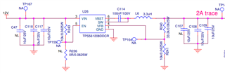
We are using TPS561208DDCR to convert 12 to 3.3V as shown in the schematic below.

In our use case we have noticed that the PMIC behavior of the IC changes under potted condition of the board (The potting material is poured over the entire Board).

3.3 V line with probe in AC coupling.

Switching pin waveform before and after potting

Feedback pin waveform before and after potting

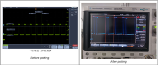
Bootstrap pin waveform before and after potting

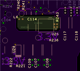
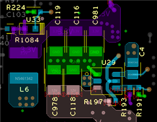
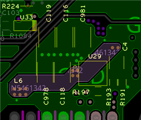
Below is the image of a potted board

This noise is impacting other sensitive ICs on the board. Can someone explain the reasoning behind the change of PMIC behaviour and how to eliminate it?

  • Hello,

    Thanks for reaching out. We will check and get back to you during these days.

    BRs

    Lucia

  • Hi Umesh,

    I want to check if only one board is potting. Do you try more boards to see if the scenario is same?

    I review your schematic and it's OK, so could you upload your layout to review? Thanks.

    Regards,

    Shipeng

  • Hi, this issue doesn't occur in 100% of the boards but happens in around 30% of the potted boards out of 200 boards checked. On the boards on which it happens, we have recreated the issue multiple times by removing and re-potting those units multiple times and similarly on multiple units. 

    Below is the layout of the U26 shown (non-relevant components have been greyed out).

    Above is bottom Layer

    Inner Layer 1 (Plane in light yellow connect the pin 2 of PMIC IC U26 to inductor.)

    Top Layer (Output trace connected to feedback resistor divider)


  • Hi Umesh,

    Your layout is not good. The SW node trace goes below the device and the Vout feedback trace, this will cause interference. When you pot boards, the parasitic capacitance gets larger and make the situation worse. So some devices cannot work normally. You need to re-layout to fix this problem.

    Regards,

    Shipeng

  • Each of these layers are separated by power planes with lots of coupling caps on power planes. Below is the stackup:

    Top

    PWR

    Inner Layer 1

    Inner Layer 2

    GND

    Bottom

    We have another board with similar schematic and layout as shown below, which has 0% of this issue and more than 200k-250k units have been produced with this layout and have been running in the field for past 4 years.

    3.3V Buck schematic

    Bottom layer

    Inner layer 2 (Plane in light purple connect the pin 2 of PMIC IC U26 to inductor.

    Inner Layer 1 (Output trace connected to feedback resistor divider)

    Stack up for the above working layout is 

    Top

    PWR

    Inner Layer 1

    Inner Layer 2

    GND

    Bottom

    Also we have tried to simulate potting parasitic capacitance by manual soldering pF caps between the components and they don't have this sort of issue.

    Our implementation is very similar to datasheet layout suggestion

    Please suggest if there could be reasons other than this.

  • Hi Umesh,

    There are something different. In your second layout, wire from SW pin to inductor doesn't go through the device and FB wire but your first layout does. So I still think it's caused by the layout. Thanks.

    Regards,

    Shipeng