This thread has been locked.

If you have a related question, please click the "Ask a related question" button in the top right corner. The newly created question will be automatically linked to this question.

TPSM365R6: layout symbol recommendation

Part Number: TPSM365R6

Tool/software:

I'm trying to make a layout symbol for TPSM365 but have some questions about the recommended footprint.

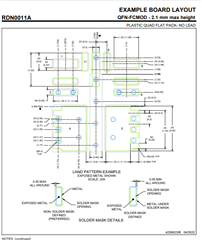
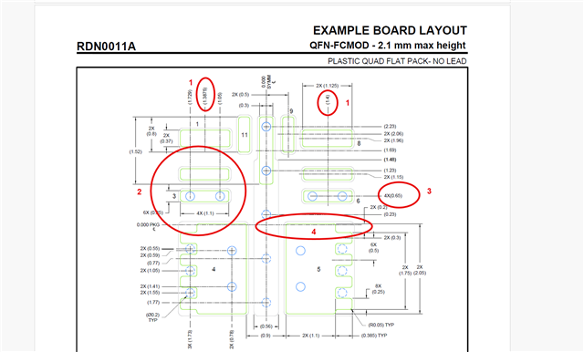
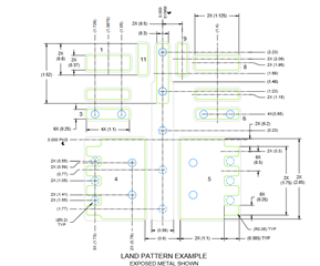
What does the gray and green indicating?

I can’t understand how we should make metal and mask for pin10(GND).

Also, I found the Ultra Librarian for this IC.(link below)

Ultra Librarian for TI

Is the above NSMD as recommended in datasheet?

  • Hello Ridge,

    Is the link below SMD or NSMD?

    Also I don't understand the reccomendded on the datasheet. what is the gray line and green line indicating?

  • Hello,

    Either one would work, but the NSMD is recommended for this device. Green represents the solder mask opening, and gray is the size of the solder mask.

    The above footprint can be used for either.

    Best regards,

    Ridge

  • Hello Ridge,

    We are developing with this device and have the same question as Emiko.

    Please reconsider your answer.


    We think the drawing is incorrect and requires updating. This is because the the pads in the "land pattern example" do not match the pads in the "solder mask details" section.

    According to the "solder mask details" drawing:

    - NSMD pads should have a solid blue inner line (to indicate metal) and a dotted green outer line (to indicate the solder mask opening).
    - SMD pads should have a solid green inner line (to indicate the solder mask opening) and a dotted outer line (to indicate the metal under the solder mask).

    However the "land pattern example" has pads drawn with solid grey outer lines and solid green inner lines. This does not match either of the "solder mask details" pad drawings.

    We suspect that pads 4, 5 and 10 should in fact be SMD, and the rest NSMD. 

    Please also note that pads 2, 7, and 10 and not labelled in the drawing and should be.

    Please refer to solder mask detail of TI RDX0007A for an example.

    Thanks,

    Gerry

  • Hello

    I will contact our product engineer team and get back to you as soon as possible.

    Thanks

  • Hello

    Here is the response from our Package team:

    Customer is asking for pin 10 design.

    So I put our PCB land pattern recommendation as below:


    The grey area is the pad and the green area is the solder mask opening.

    "land pattern example" has pads drawn with solid grey outer lines and solid green inner lines.

    Thanks

  • Hello,

    Please can someone engage with the detail of this request.

    To summarise:

    The "land pattern example" has pads drawn with solid grey outer lines and solid green inner lines. This does not match either of the "solder mask details" pad drawings.

    We suspect that pads 4, 5 and 10 should in fact be SMD, and the rest NSMD. 

    Please also note that pads 2, 7, and 10 and not labelled in the drawing and should be.

    We think the drawing is incorrect and requires updating. 

    Thank you.

  • Hello

    I will forward this to our package engineer and get back to you as 

    soon as possible.

    Thanks

  • We agree with all of Gary Hawkins comments on the drawing that urgently require clarification and in addition would also like confirmation on:

    1. Pads 8,7 & 6 on RHS are detailed as X co-ord 1.4mm from centreline origin BUT LHS pad 1 shows 1.3875mm – Does that apply to pads 2 & 3 as well as the dotted dimension line doesn’t extend down through pad 2 & 3 centres? This suggests the device isn’t symmetrical which is a bit suspect to us?
    2. The green line suggests Solder Mask Defined pad of 0.25mm wide and you replied to Gary that the grey was the pad so giving a 0.35mm wide pad. With a “vertical” pad to pad spacing of 0.5mm this would result in a 0.15mm pad edge to pad edge “gap” between pads 2 & 3 and 6 & 7. In PCB manufacture, to allow for your recommended 2 ounce copper on the top layer, the PCB manufacturer would have to etch compensate the pad by an absolute minimum of 8 mil (0.203mm), so with a gap of 0.15mm this is NOT possible, the top copper could only be 1 oz finished IF the pad is to be 0.35mm wide?
    3. I believe this note should state 6 x (0.65) i.e. 4 off vias and 2 off pads.
    4. I can’t see a dimension where the offset from the 0,0 origin point to the “top” of pads 4 & 5 is defined nor a dimension this can be derived from (ideally would like to see dimensions in both X & Y axis to the centre of the pad).

    As Gary pointed out, I also believe that with pads 1,2,3,6,7,8,9 & 11 the green colour should be changed to blue to be the required pad size for NMSD (preferred), and the grey outline be green dash to show resist oversize.


    Copper Weight Minimum Spacing Rules

    Cu Weight

    Min. Recommended Space between Copper Features and Min. Trace width

    1oz

    3.5 mil (0.089mm)

    2oz

    8 mil (0.203mm)

    3oz

    10 mil (0.254mm)

    4oz

    14 mil (0.355mm)

  • Hello

    Thank you for your patience.  I have contacted our package team.

    Thanks

  • Hello

    This issue appears to be closed.

    Thanks