This thread has been locked.

If you have a related question, please click the "Ask a related question" button in the top right corner. The newly created question will be automatically linked to this question.

UCC21550: Half bridge circuit with UCC21550 not working

Part Number: UCC21550
Other Parts Discussed in Thread: UCC28056

Tool/software:

Hi, 

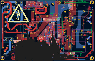
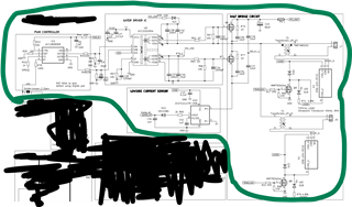
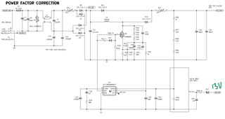
The circuit is a half bridge circuit driven by a UCC21550BQDWRQ1 isolated gate driver to drive an ultrasonic transducer load 60W, 40kHz. The circuit has a PFC UCC28056BDBVT. Attached are the schematics and PCB layout. There is no rectifier needed as a sine wave is required at the output to drive the ultrasonic load. The filter consist of a single LC network.


The primary concern is the half bridge circuit.

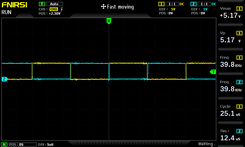
The test with no load (no transformer connected as the relay is OFF):

  • The UCC21550BQDWRQ1 input PWM was supplied by UCC28086DR.
  • The low power side was supplied by 5V DC
  • The Isolated side of UCC21550 by external regulated power supply of 13.5V DC
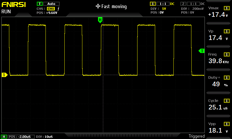
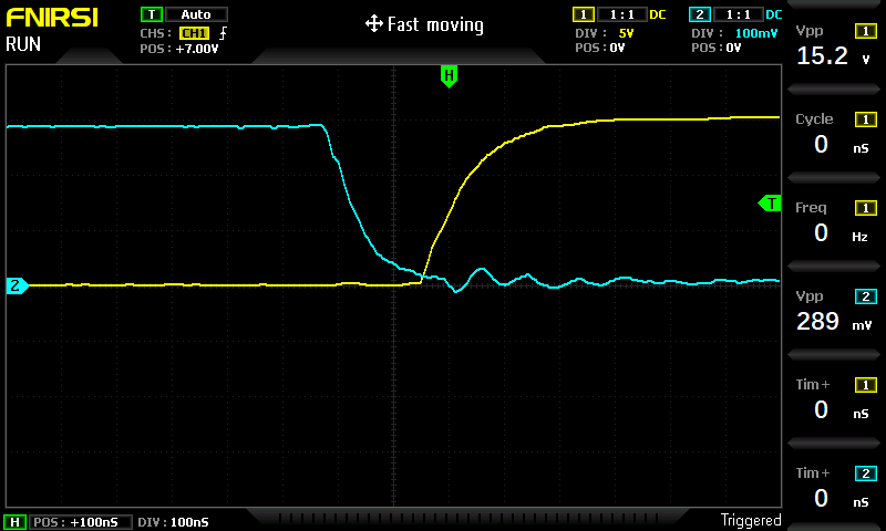
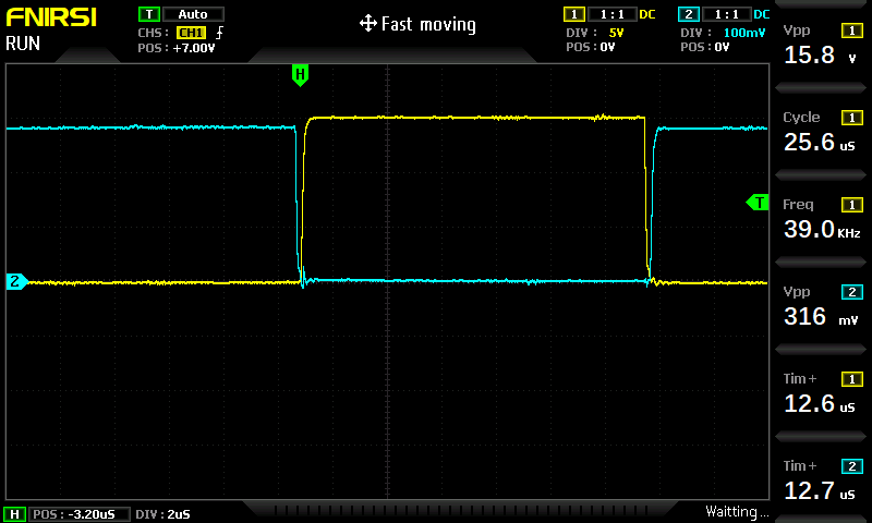
  • The PWM output both on the INA, INB (5V, 0V) and OUTA and OUTB (13V 0V) showed the expected voltage values.
  • The Input power was initially 385V DC, the PFC output and it was working fine.  The Bulk capacitor is charged up to the input voltage before turning ON the UCC21550.
  • The circuit have two inrush current limiters. 1) after the common mode choke and at the output of the PFC circuit.


Issue:

  1. The 2A fuse close to the Bulk capacitor of the half bridge circuit was connected in order to supply the PFC output voltage of 385V DC to the Input of the Half bridge circuit.
  2. Upon activating the UCC21550 IC, the 3A fuse connected to the input power supply from the mains blew, damaging the sense resistors of the PFC UCC8056 circuit and the VCC power to the PFC.  Both the PFC UCC28056BDBVT and the UCC21550 IC shared the same external power supply. But the 2A fuse connected before the Bulk capacitor of the half bridge circuit was unaffected.   Only the PFC UCC28056B was affected.
  3.  
  4. The PFC UCC28056B circuit was remove from the board. The UCC21550 circuit INA, INB and output A and B was tested without input power supply, and it worked fine as expected.
  5. Since, the PFC UCC28056 circuit was removed, the input power 332V DC (240VDC without load) is then supplied directly to the half bridge.
  6. Upon activating the UCC21550 IC, the 2A fuse connected before the Bulk capacitor of the half bridge circuit blew immediately but the replace 3A fuse from the mains did not blow up.
  7. The Drain and source of both the high side and low side MOSFET of the half bridge  were shorted, indicating that the MOSFET is damaged. The MOSFET was tested before being mounted on the PCB.


Question:

  1. What could have gone wrong with the half bridge design?
  2. Kindly review the schematic, especially the PCB layout  and give a definitive reason why it may have failed. I can send the source file (kicad) on a private chat. 


Kind regards

Bright

  • MOSFETs: SIHP24N80AE-GE3

    Inrush current limiters: B57235S0509M000

    PFC output caps: EKXL451ELL680MU35S

    Bulk capacitor  EKXL451ELL820MM25S

  • Hi Bright,

    Your schematic and layout pertaining to the gate driver portion both appear to be designed properly. To better help discover any potential root causes that may be resulting from the gate driver, do you mind sharing any test waveforms you may have saved or are able to replicate when running these tests? This may help to indicate what exactly is causing each of the fuses to blow.

    Best regards,

    Will

  • Hi Will,

    The only waveform would be from the UCC21550 gate driver output.

    The isolated side is supplied with 14V.The issue now is that the OUTA of the UCC21550 gate driver is not switching, it shows a stable 12V. The OUTB is switching properly- showing 15V ON, OFF. The INA and INB are supplied with PWM and it is working properly. I have removed all the components leaving only the non isolated resistors and caps.   I have changed the UCC21550 IC three time now but the OUTA is not switching. But the OUTB works fine. The OUTA shows 12V only when referenced with VSSB but with VSSA it shows nothing. 

    What could be the issue?Unamused

    Kind regards,

    Bright

  • Also, When the UCC21550 Is powered ON, is there meant to be any continuity between VSSA and OUTB  and between VSSA and VSSB (Ground reference)? 

  • Could it mean that the Isolation barrier was broken during the soldering?  But no continuity concerning the above mentioned with the circuit is turned OFF. 

  • I suspect that the isolation barrier between VSSA and VSSB was damaged during soldering with a heat gun. What is the recommended heat gun temperature?

  • Hi Will,

    Please ignore the hot gun temperature question

    If you are satisfied with the schematic and PCB layout, I suspect that the circuit blew up because of the deadtime between the High and low side MOSEFT, both shorted and it blew the 2A fuse. The gate resistor is 10 ohm which might be too small. I will replace the components and start with 30-40 ohms gate resistor to ensure sufficient dead time between them and to avoid shorting the circuit and send you the waveforms within a week. What do you recommend? 

    Kind regards

    Bright

  • Which one should I change?  DT value on the UCC21550 IC or the gate resistor or both?

  • Hi Bright,

    For your deadtime resistor, it will program the deadtime to reflect the following equation:

    tDT (in ns) = 8.6 * RDT (in kΩ)  +  13

    The resulting deadtime value will fall within roughly +/- 10% of what is calculated. This equation will help you determine the necessary deadtime resistor for your application.

    As for the gate resistor, that will have a much more significant effect on the output drive current. I would start here to better determine if you needed a larger gate resistor. UCC21550 is capable of driving up to +4A/-6A output current, so increasing the gate resistor will help to prevent the output current from exceeding your fuse ratings. You can utilize these equations in the UCC21550 datasheet (page 26) to help calculate the gate resistor necessary to limit your output current below your fuse ratings:

    --------------------------------------------------------------------------------

    Best regards

    Will

  • Hi Will,

    Thank you for the response. 

    I need further clarity:

    1) Did the fuse blow up because of the output current of the gate drive? or

    2) Did it blow up because of the small deadtime that may have not allowed sufficient turn OFF of the HIGH side before turn ON the LOW side, thereby shorting both High side drain and Lowside source?

    Kindly give further explanation on the possible culprit in this instance 

    Kind regards,

    Bright

  • Hi Bright,

    1. The output current of your gate drive will be calculated with the above equations, where I_OA+ is the output source current at channel A, and I_OA- is the output sink current at channel A. If your calculations do not exceed the ratings of your fuses, then the output current of the gate driver is not responsible for the fuses blowing.

    2. In terms of deadtime, make sure you have calculated the right deadtime necessary to ensure there will not be a short when the other channel is turned on. This will depend on the specs of the components used in your output power stage. Then once you have a minimum deadtime value needed, use the following equation to calculate the necessary resistor value to produce that minimum deadtime value:

    tDT (in ns) = 8.6 * RDT (in kΩ)  +  13

    In this equation, do take note of what each variable's units are. The resistor value you calculate should be within the range 1.7kΩ - 100kΩ.

    Best regards,

    Will

  • Hi Will,

    I have a question regarding the boostrap capacitor. Does it experience the DC link voltage at any point? or just the VDDA voltage, which is about 20V DC applied, in this case a cap rated 50V should suffice? or Do I need to account for DC link voltage + gate voltage for the boostrap cap?

    Kind regards,

    Bright

  • Also, does the bootstrap diode have to be rated to the DC link voltage (300V DC for example) or the VDDA voltage (20V)?

  • Hi Will,

    Please ignore the recent question. I found the answer. Bootstrap caps 2x VDD, while the bootstrap diode x1.3-1.5 the DC link. 

    Kind regards,

    Bright

  • Hi Bright,

    It seems like you were able to find an answer to your questions. Thanks for reaching out!

    Best regards,

    Will

  • Hi Will, 

    Everything was working fine before the fuse blew upon supply DC link voltage 332V DC, I have have started with 20V DC.

    After the incident, I have replaced all the components, IC, bootstrap capacitors and diode. 

    • The VDDA and VDDB is 16V (The same power supply)
    • Gate resistors 100 ohm
    • DT 20k

    The OUTA is not switching but the OUTB (Waveform attached ) is switching properly. The INA and INB signal are switching. The waveforms are attached The bootstrap capacitor and diode are correctly sized and soldered. The IC and capacitors and diode have been replaced multiple times but the OUTA is not still switching. There is continuity between the cathode of the diode and the capacitor.

    1)What could be the issue with OUTA? Bearing in mind that I have replaced the IC up to 3 times. Unamused

    Kind regards,

    Bright

  • I have changed the IC again but still the same issue. The Issue is not the IC as it is the 5th IC changed. 

  • Hi Bright,

    Thank you for sharing this information. Your dead time programming is working properly, so it is not a factor in why OUTA is not switching. At this point I would recommend you look into the schematic and layout of the output power stage. I am only able to answer questions pertaining to the schematic and layout of the gate driver and its necessary components, and everything appears to be correct with your gate driver circuitry, which is backed up with your B channel behavior.

    The only final thing I would recommend you check is regarding the continuity of the diode and capacitor. I would double check any nearby components to make sure nothing is interfering with those parts, and also check if there is a short somewhere on your board.

    Best regards,

    Will

  • Hi Will,

    Thank you for your response. 

    There are no shorts in the circuit, otherwise OUTB wouldn't not work. I have changed the boot strap diode and resistor  but no signal. 

    The VGS with reference to VSSA shows no signal but it shows 14.4V with reference to VSSB (GND).

    What really is the issue here with the OUTA? SobSob

    Kind regards,

    Bright

  • Bright, it is a holiday in the US this week, so responses will be delayed. Our team will get back to you early next week.

    Regards,

    Daniel

  • Hi Will,

    Apparently I forgot that the OUTA requires at least the Lowside MOSEFT to be connected for it to turn ON/OFF using the Bootstrap capacitor that will charge through the lowside MOSFET when turned ON (connected to ground)Sob

    DT = 20k, Gate resistor 10 ohm, VDDA and B,14V

    Waveform is attached below. 

    1) From the waveform, do you reckon 200ns deadtime gives a sufficient margin to prevent shoot through while keeping the circuit functioning efficiently?

    2) or should I used DT 50k, 440ns?

    The CH2 is differential probe x50 = 14V/50 = ~280mV

    Kind  regards,

    Bright 

  • Hi Bright,

    I hope your weekend went well. I'm glad you were able to figure out the issue regarding OUTA!

    Your dead time configuration appears to be sufficient. Programming dead time to be twice as long as what you currently have will certainly prevent shoot through, but it will result in a notable decrease in efficiency. I would definitely recommend taking multiple samples of data, to get a better understanding of the "worst case" in terms of potential shoot through. If your configuration gives enough time to prevent shoot through in the "worst case," it will be good for your application.

    Best regards,

    Will

  • Hi Will,

    The application is ultrasonic cleaner. 

    I am testing the circuit without load. I have reach 50V DC, the voltage spike (ringing) across the drain and source of High side is almost double of 50V. The MOSFET are getting really hot (no fan cooling yet). Perhaps the  400ns dead time contribution to the power dissipation is not significant?

    Previous incident: I suspect that at 332 DC link, the voltage spike may have exceeded the MOSFET drain-source voltage, leading to avalanche breakdown and short circuit. 

    Any comment would be appreciated. 

    Kind regards,

    Bright

  • Hi Bright,

    I would definitely double check your MOSFET specs to make sure it is not being used past its ratings. The dead time should be plenty, but you can certainly increase the resistor if you feel it is necessary.

    Best regards,

    Will

  • Hi Will,

    The MOSFET is sihp24n80ae, 800V

    Heatsink is HSEB20380040H01

    Increasing the gate resistor will slow the turn ON/OFF. What value would be a step up?

    Kind regards,

    Bright

  • Hi Bright,

    Feel free to check the datasheets on those, as I am only able to give recommendations on our gate drivers. In terms of your question regarding the gate resistor, could you provide some more clarification? If you're looking for a faster turn on/off time, you can decrease the gate resistor, although we recommend you keep it within the recommendations stated in our UCC21550 datasheet.

    Best regards,

    Will

  • Hi Will,

    Thank you. 

    What's the recommended gate resistor? 1-10 ohm?

    Kind regards,

    Bright

  • Hi Bright,

    For R_ON and R_OFF, you can follow the equations on page 29 of the UCC2155x Datasheet. For R_GS, we recommend a resistor between 5.1kΩ and 20kΩ.

    Best regards,

    Will

  • Hi Will,

    I think you have given the resistor range for the pull down resistor for the gate and not the external resistor for the gate (R_ON, R_OFF), which I suspect is around 1-10 ohms. 

    Kind regards,

    Bright

  • Hi Bright,

    The link I sent previously to page 29 of the datasheet shows the equations which can be used to measure R_ON and R_OFF.

    https://www.ti.com/lit/ds/symlink/ucc21550.pdf#page=29

    Best regards,

    Will

  • Hi Will, 

    I was referring to the gate resistor not pull down resistor (R_ON, R_OFF)

    Kind regards,

    Bright

  • Hi Bright,

    I understand what you are referring to now. 1Ω-10Ω should be sufficient. Feel free to look through this TechNote page that further explains the gate resistor selection:

    https://www.ti.com/lit/ab/slla385a/slla385a.pdf?ts=1720473712194&ref_url=https%253A%252F%252Fconfluence.itg.ti.com%252F

    Best regards,

    Will

  • Hi Will,

    I am gradually increasing the DC link voltage by 5V, at 50V DC, the High side MOSFET temperature is 30 deg Celsius, while the Low side MOSFET (mounted on heatsink) is getting really hot, upto 70 deg Celsius, even with fan cooling, it was still rising beyon 70 degree. 

    VDDA and B is 12.7V, gate resistor 10 ohm

    1) What could be the cause?

    2) Does it have to do with the PCB layout? I have previous attached it in our conversation. 

    Kind regards,

    Bright

  • Hi Bright,

    I would first check to make sure the MOSFET is not faulty or being pushed past its limits stated in the datasheet. Then once validated, would you mind sending any waveforms you have of the voltages and current for each MOSFET, as this can potentially help to determine the root cause of any heat generation.

    Best regards,

    Will

  • Hi Will, 

    Thank you for your response, I have attached the waveform below. Let me know if its clear enough. The MOSFET is 800V, SIHP24N80AE-GE3

    Highside is blue coloured x50 probe

    Lowside is yellow coloured x10 probe. 

    Kind regards,

    Bright

  • Hi WIll,

    From the waveform above, I suspect cross-conduction risk (shoot-through) due to the partial overlap of the voltage across the Highside and the Lowside MOSFET, and led to increased current flowing through the MOSFET, implying high power dissipation.

    The PSU current limit was set to 430mA. At 40V DC, the current draw was 30mA, it showed a cleaner waveform. But when it was increase to 50V DC, the current draw reached the set limit of 430mA, the voltage on the PSU dropped to 46VDC and current 430mA. The lowside MOSFET temperature immediately spike up beyond 70 deg Cel and was increasing before I deenergised the circuit. 

    I suspect the risk of cross conduction  is heating up the Low side MOSFET and the overlap, due to the increased resistance at the drain-source when operating in its linear region (partially turned).

    1) What do you think? 

    2) How can it be rectified?

    Kind regards,

    Bright

  • Hi Bright,

    It appears that there could potentially be shoot-through involved. Increasing the dead time could fix this issue. Let me know if your system continues this behavior after increasing the dead time.

    Best regards,

    Will