This thread has been locked.

If you have a related question, please click the "Ask a related question" button in the top right corner. The newly created question will be automatically linked to this question.

LM5176: LM5176 Dead Time issue

Part Number: LM5176

Tool/software:

Hi,

Based on LM5176EVM-HP schematic to design LM5176 12V buck 5V.

But we found that the dead time was 45ns and may lead to the risk of MOSFET shut-through or blow up.

How to adjust deadtime? 

Regards

Hins Weng

  • Hi Hins,

    The first plot shows a very slow slope for the gate signal of the high side Buck  MOSFET.

    From a pure math this would give a Gate charge of the MOSFET of 22uC which can not be.

    Do you have any gate resistor added?

    The dead time can be seen in the scope plot to be around 45ns but the driver does not get the gate low in a reasonable time

    Also the peak on SW1 before going down looks somehow weird and not sure where this is coming from - might the SW2 but not sure

    Can you also let me know what channel shows what in the second plot - colors are different to the first one so not sure how the mapping is here.

    Best regards,

     Stefan

  • Hi Stefan,

    No, do not have to add any gate resistors, the value is 0 OHM.  But I tried adding a 2.2 OHM resistor to LDRV1 gate, but there was no change. 

    For the second plot - add the channel information for your reference.

    The peak value on SW1 seems to start from BOOT 1 before it falls. And it was checked with SW2, and it looks very stable.

    Moreover, HDRV1 is going down, but LDRV1 starts to go up. 

    Regards

    Hins Weng

  • Hi Hins,

    i checked internally and the waveform here is the expected one. 

    The dead time is from start of falling HDRV1 to rise of LDRV1.

    You can also see that the high side has already reach the off level before the low side starts to conduct.

    If you would like to add some additional dead time you can add a Gate resistor with an parallel diode in reverse direction.

    This would slow down the turn on and have a fast turn off.

    Best regards,

     Stefan

  • Hi Stefan,

    Do you mean the original waveform is normal? 

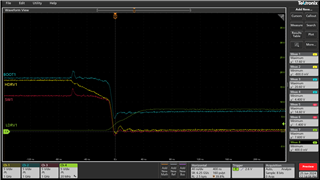
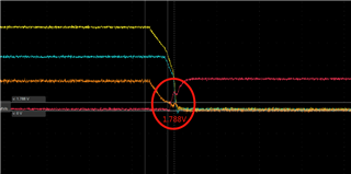
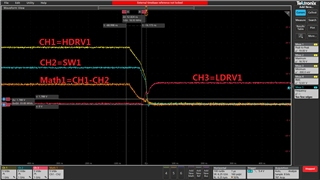
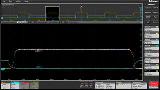
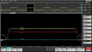
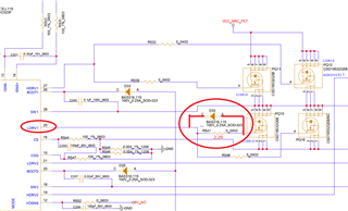
    I mean, before HDRV1 reached its lowest level, LDRV1 had already risen, and the intersection point was between 1.7V and 2.4V. At this point, the high side and low side MOSFETs are turned on at the same time, which is easy to cause MOS burning. 

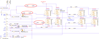
    So I want to delay the rise time of LDRV1 until HDRV1 has been completely reduced to a minimum.  To add a Gate resistor with a parallel diode in reverse direction, is the screenshot right? 

    Regards

    Hins Weng

  • Hi Hins,

    before the low side gate signal starts to rise, the high side gate signal has reached a level of 1.78 V.

    At this level the MOSFET has already shut off:

    The schematic is right but just to mentioned it, it also needs to be added on the second MOSFET

    Best regards,

     Stefan