This thread has been locked.

If you have a related question, please click the "Ask a related question" button in the top right corner. The newly created question will be automatically linked to this question.

TPS54140: About AC analyze Split-Rail topology

Part Number: TPS54140

Tool/software:

Hi team,

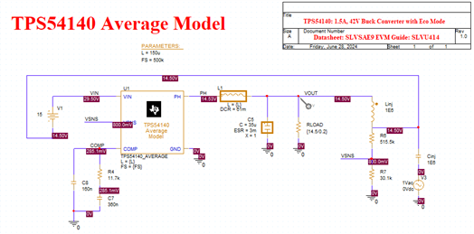
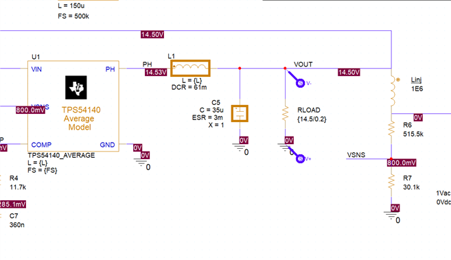
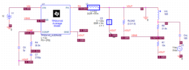
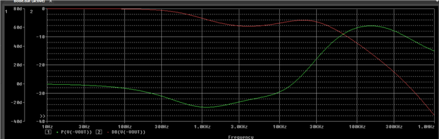
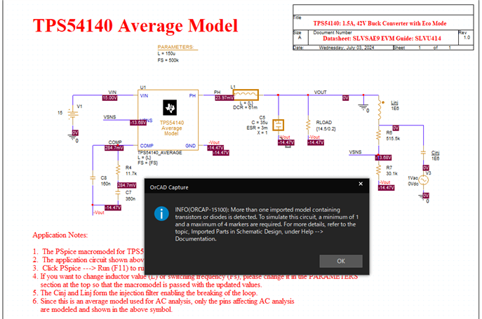
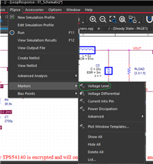
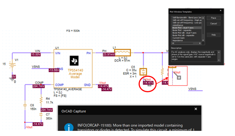
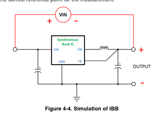
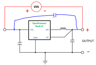
Our customer want to AC analysis by TPS54140 PSpice Average Model to Split-Rail topology.

They want to check Bode plot on setting value of result of calculate tools(SWIFTPOSNEG-CALC-v4).

Is it possible by this model?

Or are there other way of AC analysis in the case using this device as Split Rail topology circuit? 

Best regards,

teritama

  • Hello,

    When simulating inverting designs without a dedicated IBB model, please follow the recommendations in Section 4.4.3 of this application note: https://www.ti.com/lit/an/snva856b/snva856b.pdf

    Best regards,

    Ridge

  • Hello Ridge-san,

    Thank you for the information. Please answer below question too.

    How I decided Cinj and Linj value?

    Is it okey that Output voltage setting resistance(R6, R7) is same value with Split-Rail circuit? These resistance is connected between positive output line and negative output line.

    Best regards,

    teritama

  • Hi Teritama-san,

    In simulation you don't need to setup the same measurement network as in Figure 4-2 of the application note for an AC analysis. That is an example of using a network analyzer on the bench where you would need an injection resistor in the feedback path.

    The resistors for feedback are calculated the same as with the buck topology. 

    Best regards,

    Ridge

  • Hi Ridge-san,

    Thank you for reply.

    I set up like below figure for Vin=15V, Vout=±14.5V condition reference Application note Section 4.4.3 you shared.

    Best regards,

    teritama

  • Hi Teritama-san,

    That looks like the correct setup. You may not need the Cinj and Linj for AC analysis. 

    When you measure the output, make sure to use the differential probe and reference all of your measurements to the Vout node. Since Vout is now the system GND in IBB, you need to use that as the reference point so that you see the correct voltage values.

    Best regards,

    Ridge

  • Hi Ridge-san,

    Thank you for your checking.

    >You may not need the Cinj and Linj for AC analysis. 

    ⇒In my understanding, Cinj and Linj is needed to inject the AC sweep signal. If don't use Cinj and Linj, how I connect Vac? 

    >When you measure the output, make sure to use the differential probe and reference all of your measurements to the Vout node.

    ⇒This means like below plot. Right?

    Best regards,

    teritama

  • Hi Teritama-san,

    I spoke to the team regarding your questions on AC analysis, and this model is not compatible with AC analysis. We do not have an AC PSPICE model for this device. To assess stability, the next best thing would be to perform a load transient test and check the output for a stable response. 

    Your measurement probes are setup correctly.

    Best regards,

    Ridge

  • Hi Ridge-san,

    >I spoke to the team regarding your questions on AC analysis, and this model is not compatible with AC analysis. 

    ⇒In my understanding, average model is for AC analysis model. This means average model doesn't support IBB(Split-Rail) topology?

    Best regards,

    teritama

  • Hi Teritama-san,

    With the IBB configuration the AC analysis model may not function properly with the way it is setup. Since the internal GND connections of the model are not floating, it is not possible to set them up as you would on a PCB when configuring the IC for IBB. As a result, the simulated AC response of the system may not accurately represent results on the bench. 

    I think the best option would be simulating a load transient response with the transient model. We can also help to review your design schematic as well if you can share it. Just to confirm, are you designing for a split rail or just one inverting output? The PSPICE schematic looks like a single output IBB rather than split rail.

    Best regards,

    Ridge

  • Hi Ridge-san,

    >Just to confirm, are you designing for a split rail or just one inverting output? The PSPICE schematic looks like a single output IBB rather than split rail.

    ⇒As the thread title shows, the customer is designing split-rail topology. I used the IBB schematic because follow recommendation in in Section 4.4.3 of this application note: https://www.ti.com/lit/an/snva856b/snva856b.pdf you shared before.

    As the thread first question, they want to know how to simulate the bode plot by Split-rail topology. And I guessed it maybe possible by Pspice average model at first.

    Is it possible on the Pspice for TI?

    Best regards,

    teritama

  • Hi Teritama-san,

    Here you can see the device correctly simulated a negative voltage, but I get some unintelligible data on the bode plot.

    It may be easier to simulate a load transient instead.

    Thanks

    Andrew

  • Hi Andrew-san,

    Thank you for your support. I tried your reference your schematic. But the simulation is failed by ERROR like below figure.
    Please tell me about reason of this ERROR?

    >It may be easier to simulate a load transient instead.

    ⇒Does this mean recommend to use transient model and evaluate by transient response like the way suggested in this application note https://www.ti.com/lit/an/slva381b/slva381b.pdf ?

    Best regards,

    teritama

  • Hi Teritama-san,

    On PSPICE for TI you need to place at least 1 marker in order for it to simulate.

    Yes, the app note you listed is good.

    Thanks,

    Andrew

  • Hi Andrew-san,

    I used Bode plot - Dual Y axes. Is this marker not a pertinent marker?

    >Yes, the app note you listed is good.

    ⇒I understand, When evaluate IBB topology circuit. Is this okey that the simulation circuit follow the recommendations in Section 4.4.3 of this application note: https://www.ti.com/lit/an/snva856b/snva856b.pdf?

    I have a concern regarding Section 6 General Considerations in the application note.

    Are there some way of I know about the model internal GND?

    Best regards,

    teritama

  • Hi Teritama-san

    Hmm maybe just put a couple of simple voltage marker on it. PSPICE for TI is a bit finicky.

    If I hook up the pspice like this I get errors, so I wouldn't recommend doing it like that.

    Thanks,

    Andrew

  • Hi Andrew-san for TI. 


    Thank you for supports. I understand that this topology is not recommended for Pspice model.

    I would suggest to the customer to evaluate on the bench mainly.

    Best regards,

    teritama

  • Hi Teritama,

    It can be ok sometimes for transient simulation, but yeah the easiest way would be to test in the lab.

    It might be easiest to use the EVM, and connect the power supply like this. (you need to add additional blue capacitor).

    However, I'd start at low voltages and current limit the supply, so that nothing blows up.

    Thanks,

    Andrew

  • Hello,

    Since we have not head back in a while, I will be closing this thread. If you have more questions, you can open a new thread or re-open this one by replying. 

    Best regards,

    Ridge