This thread has been locked.

If you have a related question, please click the "Ask a related question" button in the top right corner. The newly created question will be automatically linked to this question.

UCC21750: Trying to find a non isolated gate driver with desat protection

Part Number: UCC21750
Other Parts Discussed in Thread: UCC57102, UCC57108

Tool/software:

Hi

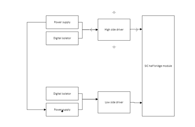
Can i please know whether you have a gate driver with following requirements. 

  • Power device- SIC.
  • Non Isolated

  • Has Desaturation protection option.
  • Miller clamp.

Basically an SIC gate driver similar to UCC21750, but without isolation. 

Regards

  • Hi Damith,

    Can you please share, what is the end Application? 

    Thanks

    Sasi

  • Hi Damith,

    The UCC57108 (8V UVLO) and UCC57102 (12V UVLO) are our non-isolated, low-side gate drivers that have desaturation protection. Currently, none of our non-isolated drivers have Miller clamping built-in to the driver.

    Like Sasi asked, can you share the application for this request?

    Thanks,
    Rubas

  • Thanks for the suggestions Rubas.

    Hi Sasikala.

    Idea is to create a gate driver with more than 15mm clarence ( 15mm clarence is set by the standards we follow ). Since none of your gate drivers doesn't match that clearance, only option is to use a 15mm digital isolator from your arsenal along with a low side gate driver. But that gate driver should have all the basic protection functionalities and the drive strength in the UCC21750, which are soft turn off, desaturation detection and at least 10A source sink current capability. 
    But looks like its impossible at the moment. 
    Another thought. Is it ok to power both sides of the UCC21750 with the same power supply. So effectively, we can use all the functionalities while getting rid of the isolation barrier, which we don't need. 

    Regards
    Damith

  • Hi Damith,

    Thanks for the detailed note. yes you can make use of UCC217xx family of devices and can treat as non-isolated by connecting both grounds. However we need to understand your system little better.

    I believe that you are planning to have Gate driver at the isolated side close to the FET and connecting GND and COM together. Is my understanding right? is it possible to share the block diagram to show your implementation approach?

    Another thing I am curious about what end application needs such high clearance. It may give us to investigate more and plan such devices in the future.

    Looking forward for your inputs to provide effective solution.

    Thanks

    Sasi

  • Hi Sasikala

    Thanks for the clarification. 

    Here are some more details. 

    We are designing according to UL61800-5-1 11/02/2021. 

    Here are our specifications. 

    Bidirectional DC DC converter. 

    Secondary side voltage after rectification- 1300V DC
    Over Voltage category- 2
    Pollution degree-1
    Isolation- reinforced isolation from HV to ground. 

    Its this reinforced isolation makes the clearance high. 


    Regards
    Damith

  • Hi Damith,

    Thanks for the detailed explanation.

    Though UCC21750Q1 family doesn't have wider package, it has reinforced isolation with working voltage of 1500V Vrms.

    It has the following isolation certification: DIN EN IEC 60747-17 (VDE 0884-17). Not sure if it can fulfill for your application. I would like to highlight the isolation capability of UCC21750Q1.

    Thanks

    Sasi

  • Thanks Sasikala

    Its the external PCB clearance that we cannot get around. External PCB clearance is limited by the Package clearance. 

    Regards
    Damith

  • Hi Damith,

    Understood, yes you could use UCC21750- even basic isolation (without Q1) as you are planning digital isolators on top of the gate driver. Yes you can short COM and GND and get the gate driver working. However I would like to review the block diagram view of how the gate driver is positioned with respect to HV and LV side. Is it possible to share the details? So that we are not missing any unknown, as this is not typical use case.

    Really appreciate your detailed, quicker responses.

    Thanks

    Sasi

  • Hi Sasikala

    This is a very crude representation of the intended design. Left hand side is the controller side. Right hand side is the HV side. it has both high and low side gate drivers. Both are completely isolated from each. 


  • Hi Damith,

    Thanks for sharing the block diagram view. Yes you can connect GND and COM. It should work. However please ensure that the power ground noise is separated from the device ground. So don't plan one big ground plane between IC ground and the power plane. Maintain high current path separately and connect the IC ground like sense line. Also plan decoupling caps on all the supply pins, INP, INN, EN/RST pins very close to the device pin.

    Hope it helps.

  • Hi Sasikala

    Thanks for the confirmation and heads-up. I will keep that in mind. Since we are using SIC 62mm modules, it has a kelvin connection anyway. Therefore power path wont interact with signals, i guess. 

    Regards
    Damith.