This thread has been locked.

If you have a related question, please click the "Ask a related question" button in the top right corner. The newly created question will be automatically linked to this question.

TPS552872-Q1: BMS

Part Number: TPS552872-Q1

Tool/software:

Hello Experts,

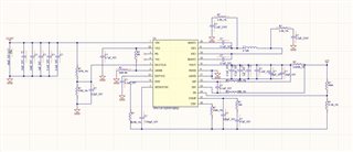
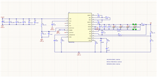
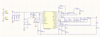
I am going to use TPS552872Q IC as my Buck Boost Converter in my BMS project, following are the preset values:

Input Voltage Range = 09 - 32V

Output Fixed voltage = 12V

Max Output Current = 2A

Switching Frequency = 300kHz

Efficiency = 98%

Enable voltage = above 1.2V
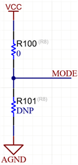
In Auto PFM mode

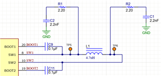
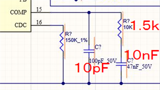
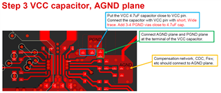
Kindly verify the Schematics and let me know

/resized-image/__size/320x240/__key/communityserver-discussions-components-files/196/pastedimage1719565592745v1.png

  • Hi Abhiram,

    Thanks for reaching out.

    1. May I know how is this Buck-boost is used here? Do you have any block diagram about this?

    2. In automotive applications, FPWM mode is usually selected due to fixed switching frequency and is easier to pass EMI. May I know the reason to choose PFM?

    3. What is the part number of the inductor?

    4. What is ESR value and part number of the output capacitance? Then we can check COMP parameters.

    BRs,

    Bryce

  • Dear Bryce, 

    Thanks for your suggestion.

    1. This buck boost is used to power one of our gateway IC and further 5V LDO's.

    2. We had selected APFM as our BMS is going to use on different power levels in i.e., sleep and standby. As per you suggest we can switch to FPWM.

    3. SRN8040TA-5R6MCT-ND (5.6uH inductor we are going to use). It is of Bourns.

    4. EDH226M050S9GAA is the 22uF Electrolytic capacitor.

    Thanks 

  • Hi Abhiram,

    Thanks for feedback. Please find my replies below.

    1. If BMS is used on sleep and standby applications, is the efficiency important for the system? Because the efficiency at light load with FPWM would be lower than PFM mode. Or it is suggested to modify the MODE pin as below to leave the options to select PFM or FPWM according to the real final test results..

    2. Check the effective capacitance of VCC cap is higher than 2uF at 5.2V dc bias voltage. And recommend to add one 0.1uF/0402 close to VCC pin.

    3. Recommend to change Fsw to 400kHz to pass the EMI test easily according to the EMI test standard.

    4. If fsw=400kHz is selected, the inductor value can choose 4.7uH with saturation current>4A.

    5. Recommend to change the output current sense resistor to 20ohm to set 2.5A output current limit since 2A is the max output current.

    6. Recommend to add two 10uF ceramic capacitors at the output side to decrease the output voltage ripple. 

    7. Recommend to add RC snubbers (2.2ohm---1206 package)+2.2nF at both SW1 and SW2 node for EMI consideration, you can leave them floating first and populate them according to the EMI test results.

    8. For the COMP parameters, I don't find the ESR value of EDH226M050S9GAA on the official website, can you share the value with me? And the ESR value at -40C is also important because we saw some capacitors have very large ESR at low temp and would cause the system unstable.

    BRs,

    Bryce

  • Hi Bryce,

    Thanks for your suggestions, 

    We will follow the same.

    We are going with 10uF+10uF+2.2uF Ceramic capacitors in the output Capacitor. Could you please let us know the maximum ESR we can keep in that.

    We also have one doubt that you have mentioned 20ohms sense resistor. Is it 20 mOhms because the calculated value is coming in the range of 25 mOhms.

    Rest of the circuit would be according to attached calculation sheet right

    ...

    Thanks & Regards

    Abhiram

  • Hi Abhiram,

    1. Do you mean the output capacitors will change to only 2*0.1uF+1uF+2.2uF+2*10uF and all are ceramic capacitors? Can you share the screenshot with us and share the part number of the output capacitors with us? For ceramic capacitors, the ESR is very small compared with aluminum capacitors, the ESR is not critical.

    2. Since you mentioned the max output current will be 2A, it is recommend to select higher output current limit value to leave some margin.

    BRs,

    Bryce

  • Hi Bryce,

    PFA sent for your reference.

    IC part number - TPS552872-Q1

    TPS552872-Q1

    Also, kindly clear a doubt that you have mentioned 20ohms sense resistor. Is it 20 mOhms because the calculated value is coming in the range of 25 mOhms.

    Thanks & Regards,

    Abhiram

  • Hi Abhiram,

    1. The 20mohm sense resistor is recommended because you mentioned the max output current would be 2A. If you use 25mohm here, the output current limit value would also be 50mV/25mohm=2A, which means you could trigger the output current limit protection at the max loading 2A. So recommend to choose smaller Rsense to leave some margin for output current limit protection.

    2. Recommend to add one 0.1uF/0402 cap close to VCC pin.

    3. Check the saturation current of the inductor is larger than 4A.

    4. Recommend to change Rcomp=1.5k, Ccomp=10nF and Chf=10pF as below.

    5. For the snubber cap at SW1 and SW2 node, 50V voltage rating is ok.

    6. More output capacitors may be needed to improve the output undershoot/overshoot voltage during load transient.

    7. Please follow the attached layout guideline and send to us for review when finished.

    3833.TPS55289 Layout Guide line.pdf

    BRs,

    Bryce

  • Dear Bryce,

    Greetings!!

    1.We have placed CRF1206-FZ-R020ELF 20mOHM (1206 package) Resistor as recommended.

    2. 0.1uF cap is placed near VCC along with 4.7uF.

    3. We have placed 4.7uhH inductor with ISAT of 5.9A (SPM5030VT-4R7M-D).

    4. Changes has been done according to your recommendation on 'Comp' pin. (Please refer the attached schematic)

    5. We have updated the voltage rating of the snubber caps to 50V for SW1 & SW2.

    6. We have added 100nF and 10nF MLCC (50V) in the output although in further circuits we have added significant input capacitors to improve the performance in load transient.

    Please find attached schematics for your review:

    /resized-image/__size/320x240/__key/communityserver-discussions-components-files/196/pastedimage1719988596493v3.png

    Best Regards,

    Abhiram Tiwary,

    Hardware Design Engineer

  • Hi Abhiram,

    Please note that for MODE pin, you need to leave R3 or R5 floating to select PFM or FPWM. Others look ok for me. 

    BRs,

    Bryce

  • Dear Bryce,

    Thank you for your kind support, we have kept the R5 as DNP and R3 as initial provision to FPWM

  • Dear Bryce,

    One more thing we need to confirm that is it essential to separate AGND & PGND with a ferrite bead

    Best Regards

    Abhiram

  • Hi Abhiram,

    Yes, it is strongly recommended to separate the AGND and PGND at the PCB to achieve the best performance of this device. Ferrite bead is not needed, just connect AGND with PGND at VCC cap ground via the net tie is ok.

    BRs,

    Bryce