This thread has been locked.

If you have a related question, please click the "Ask a related question" button in the top right corner. The newly created question will be automatically linked to this question.

LM5122: Subharmonic Current Oscillations on Power Input

Part Number: LM5122

Tool/software:

Hello,

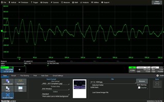
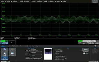
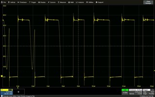
We've configured two LM5122 Synchronous Boost Controllers to work as a master/slave pair, but we're getting a fair amount of subharmonic current oscillations on the power input line. The input voltage range is from 25V to 35V and the output is set for 55V. We should be able to supply about 700W continuous, with brief peaks of up to 2000W. The oscillation amplitude is several amps peak-to-peak, of which the main component is an 18kHz sine wave at lower power levels, or a 96kHz sine wave which starts to dominate at higher power levels. Unfortunately, we are limited to only 80uF of input capacitance and 140uF of output capacitance. We were able to reduce the amplitude of the oscillations by adjusting the slope compensation K factor, and right now we have a value of 1.5 which is giving us the best results so far. The current sense resistors are each 1.5mohms, the undervoltage lockout is currently set to 20V, the Vcc caps are 10uF and the BST caps are 470nF. The boost inductors are each 8.2uH and the PWM switching frequency is set to 300kHz. The feedback compensation network parameters are as follows: Ccomp = 33nF, Rcomp = 10kohm, and Chf = 560pF.

I've attached two scope plots of the input current (AC-coupled, 1A/div) under two different load conditions (100W and 500W).

Another significant problem we're encountering is that the channels are unbalanced, with the master circuit supplying significantly more power that the slave circuit.

Regards,

Florindo

  • Hi Florindo,

    Thanks for using the e2e forum.
    Based on the given parameters, the LM5122 in two phase topology should be fit for the application. Inductance and fsw should be okay as well.
    I am concerned about the low output capacitance.
    Low output caps and an aggressive compensation network may lead to RHPZ instability. I would recommend to double check if the compensation network is stable for the given operation conditions. You can use the Power Stage Designer tool for this:
    https://www.ti.com/tool/POWERSTAGE-DESIGNER

    The inbalance of the current sharing may also be related to the oscillation of the output voltage.
    Just for debugging purposes, would it be possible to attach a large bulk capacitor to the output and see if the design runs stable then? If the instability still consists, we may need to look deeper into the rest of the design.

    Best regards,
    Niklas

  • Thanks for the prompt reply Niklas. The worst-case output voltage ripple is about 2.5Vp-p and reduces to 2Vp-p when adding a 470uF capacitor to the output, but the current oscillations on the input line are still quite large. Adding an EMI filter prior to the input reduces the current oscillations, but the instability is still present. The MOSFETs do not have snubbers at the moment, but there is the provision to have them mounted, could this reduce potential ringing that may be leading to the instability?

  • Hi Florindo,

    Thanks for the update.
    If there is still oscillation after measuring with 470uF caps on the output, I agree that the instability has another source.
    Would it be possible to take a measurement of the switch node signal?
    If there are large overshoots visible, snubbers or higher gate resistors are a good solution.
    You can also measure the VCC voltage to see if the internal control and gate driver voltage is stable.

    If you are willing to share the schematic of your design, I can also offer to review it and give feedback on possible improvements.

    Best regards,
    Niklas

  • Attached is a plot of the low-side gate drive signal (at an output load of 100W); it seems as though the duty cycle exceeds 50% every now and then. Also, there are two plots of the switch node (no load and 100W). Since we are configured in diode emulation mode, there is ringing at the switch node once the inductor current discharges and the node voltage drops below the output voltage level. Finally, the VCC voltage seems rather noisy.

  • Hi Florindo,

    Thanks for the waveform attachments.

    I agree there is some switch node ringing, but I am also concerned about the large negative overshoot on the switch node of almost -10V.
    Snubbers should be a good approach, but this may not suffice in fixing noise on VCC.

    If the noise within in the system is layout related, it is difficult to solve this on schematic level.

    I do not have the schematic or layout files available, so all of this is based on speculation, but can check double check the design for separation of analog ground and power ground? Is the power stage compact and routed effectively? Is the design using solid pads at the power stage (no thermal relief pads)?

    Best regards,
    Niklas

  • Hi Niklas,

    At the moment we have a single ground present on various layers, covering the vast majority of the PCB. Is the separation of the analog and power grounds essential? I realize that the datasheet suggests this as well.

    Florindo

  • Hi Florindo,

    It is difficult to say if it is essential. Separation of analog and power ground helps to prevent noise on the sensing signals.
    For example, if the trace of the main current flow over GND passes along the ground connection of COMP and FB, the sensing signals can indeed start to jitter, which can cause inaccuracy or even oscillation of the regulation.

    As you were not able to share any schematic or layout files to confirm the suggested root causes, I assume you are not able to communicate these files externally. If you still want the files to be reviewed, you can also contact me via private message.
    If this is also not possible, I suggest to read through some literature on desing tipps, rebuild the board and check if the behavior improves.

    Here is some additional material to check within your design:
    https://www.ti.com/lit/wp/slyy200a/slyy200a.pdf
    https://www.ti.com/lit/an/slva381b/slva381b.pdf


    Best regards,
    Niklas