This thread has been locked.

If you have a related question, please click the "Ask a related question" button in the top right corner. The newly created question will be automatically linked to this question.

TPS40345: why there is no (1-D) in equation 11 Cin(min) of TPS40345?

Part Number: TPS40345

Tool/software:

Hi, TI

How to select input capacitors for a buck converter  slyt670 How to select input capacitors for a buck converter

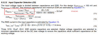
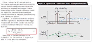
From slyt670, we know the calculation of Cin(min) is the Equation (1) with D = Vout / Vin.

But, why there is no (1-D) in equation 11 Cin(min) of TPS40345?

  •  

    The equation in slyt670 assumes there is no dynamic current from VIN over the full switching period, so the input capacitor handles only the peak - average input current across the full switching cycle and ΔVin is reduced by the average input current, which is where the 1-D factor comes from.  In most applications, this equation will produce a low minimum Cin value and higher input voltage ripple.

    The equation in the TPS40345 datasheet assumes there is no dynamic current from VIN during the ON time, but that the input voltage is able to recover each switch cycle during the OFF time, which is generally more realistic in real systems.  This eliminates the 1-D factor from the equation and produces a slightly larger minimum Cin.  In most applications, this equation will produce a high minimum Cin value and lower input voltage ripple.

    The exact minimum Cin that will produce the calculated maximum Vin(ripple) is between these two values, and depends on the dynamic impedance of the sourcing supply at the switching frequency.  Using the later equation ensures Cin is selected to that Vin(ripple) is always less than the maximum specification.

  • Hi Peter

    Thanks for your reply.

    I can understand the slyt670 equation (1) from Qon or Qoff = D*(1-D)*Io*Tsw = Cin * Delta V

    But still can't understand the tps40345 equation (11)...Could you explain this more...

  •  

    Both equations are Cin = ΔQ / ΔVin equations.  The difference is what input current each assumes at the start of the switching cycle.

    The equation in slyt670,  assumes the input current from the source is constant, with no AC ripple.  Thus the current before the On time is equal to the average input voltage I_in(avg), the high-side FET is drawing current out of the VIN node equal to IOUT during the On-time D / Fsw.  As a result, the current drawn from the capacitor is the Output current minus the average input current.

    So the ΔQ = (Io - Iavg) x D / Fsw. 

    Since Iavg = Io x D

    Io - Iavg = Io - Io x D = Io x (1-D)

    So, ΔQ = (Io - Iavg) x D/Fsw = Io x D x (1-D) / Fsw

    In the TPS40345 Equation (11), the source is assumed to have enough dynamic current that the VIN capacitor is recharged the to the source voltage during the off-time, so the input current is zero at the start of the switching cycle, removing the -Iavg component from the first equation.

    So ΔQ = (Io) x D / Fsw

    Since D = Vout/Vin, 

    thus, ΔQ = Io x Vout/(Vin x Fsw)

    In both cases, ΔQ is divided by ΔVin to calculate the minimum input capacitance and we get:


    Io x D x (1-D) / (Fsw x ΔVin) in slyt670

    and

    Io x Vout/(Vin x Fsw x ΔVin) in the TPS40345 datasheet

  • Hi Peter

    Get it.

    Another question:

    As shown in the figure below, theoretically, the IIN (input current of power source) should be only DC without any ripple current ?

    figure from Basic Calculation of a Buck Converter’s Power Stage | Richtek Technology

  •  

    I don't see a question, so I will have to infer what the question is.

    Yes, the diagram shows only DC input current with no AC ripple current, but I said that the TPS40345 equations are based on some input current ripple, with the source current returning to 0 with each switching cycle?  Which is correct?

    The true DC current with no ripple current is never actually correct.  No matter how high the source impedance is at the switching frequency, there will always be some ripple current, though it can be extremely small.  Equally, the "returns to 0 current" estimate is also never actually correct, no matter how low the source impedance is at the switching frequency, the drop from Source to VIN at the MOSFET also never actually gets to zero, though it can get extremely close.

    Let's say the local bypass capacitors are sized to limit the input ripple current to less than 250mV.  How much ΔI can that 250mV over the on-time drive from the source?  If the "source" is a local bulk capacitor bank with 4 capacitors with 25mΩ of ESR through a few inches of planar trace, that source impedance could be extremely low allowing for a lot of ripple current from the sourcing supply.  Even with 10nH of source inductance, it's possible to get 25A of AC ripple at 500kHz switching frequency.

    Now, if we move the sourcing supply much further away, or we add intentional impedance such as a ferrite bead, we can get the ripple current much lower.  That same example above, if we add a 10-ohm @ 100kHz Ferrite Bead in series with the input, the AC ripple current will drop to less than 20mA.

    For sizing the ceramic bypass capacitors to protect any bulk capacitors from excessive RMS current, it is almost always necessary to use the earlier equation, since there is rarely more than 1-2 nH of source inductance between bulk input capacitors and the ceramic input capacitors, much less a filter inductor or ferrite bead.

    Thus, the TPS40345 elects for a "worst case" design so that the results will always be better than the specified requirements.  For sizing the RMS ripple current rating of the ceramic capacitors, it assumes zero ripple current from the source, since there may not be any ripple current.  For sizing the input capacitance, it assumes there is sufficient AC ripple to reset the source current to zero, since that increases the VIn ripple if it's not accounted for.  In real circuits, the actual results are always between these two extremes.

  • Hi Peter

    Get it. thanks for your patience.