This thread has been locked.

If you have a related question, please click the "Ask a related question" button in the top right corner. The newly created question will be automatically linked to this question.

TPS2595: TPS259540DSGR Application Questions

Part Number: TPS2595

Tool/software:

Dear Designer,

My customer encountered a problem when using Ti's efuse chip TPS259540DSGR, which is described as follows.
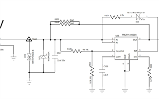
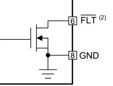
In the figure below, when J2 inputs 13.1V DC, the D20 LED light is on. At this time, the output voltage of TPS259540DSGR is 13.04V, the output function is normal, the Fault pin voltage is 11.51V, and the voltage across the LED light is 1.52V.
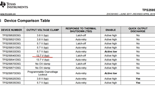
According to the specification, after the input voltage exceeds 13.7V, TPS259540DSGR will start overvoltage protection and clamp the output voltage at 13.7V. But now the input is only 13.1V, why is the LED light on?
Please help analyze the reason, thank you!

Best Regards,

Arabella Zhang

  • Hi Arabella Zhang,

    It doesn't look like fault has occurred in this system. Also, the fault pin does not go low for OVC response. 

    Since the FLTb pin is active low and is an open drain configuration, when it goes low, it goes down to 0V. Here, I can see that abs max of FLTb pin is being violated. That can be a reason for this. Please keep the pull up voltage below recommended max of 6V. 

    Click resolved if no other follow up questions or reply here.

    Best Regards,
    Arush

  • 1. Design as the schematic diagram below. We have tested that TPS259540DSGR can indicate overvoltage with LED after 13.1V, and the consistency is very good. Can you explain the principle?
    2. Our product has a need for prompt after overvoltage. LED light display is a better solution. Can you recommend a design?

  • 6V is recommended maximum and 7V is absolute maximum. It is better to keep the voltage below recommended maximum.

  • 1. They can add a resistive divider at VIN for a pull up voltage of FLTb pin. FLTb pin is open-drain pin (shown in the image)

    Also, when you mentioned "consistency is very good", Is this working as expected? OVC shouldn't trigger the FLTb pin.  

    2. If there is too much difference in Vin and Vout, the excess power will dissipate at the junction of device. This power dissipation can cause Thermal shutdown which will result in FLTb pin going low. This will also take some time between the overvoltage event happening and the shutdown. Another way is to use TPS25973 variant of this device which do not have clamp but instead have an Over voltage lock out. This will turn of the device in case of overvoltage event and FLTb will go low. And last option is to add some external circuitry which can monitor the jump in voltage levels (voltage supervisor or something similar. I will think some more and get back to you if I get some other solution)  

    Best Regards,
    Arush