This thread has been locked.

If you have a related question, please click the "Ask a related question" button in the top right corner. The newly created question will be automatically linked to this question.

TPS650864: TPS650864

Part Number: TPS650864
Other Parts Discussed in Thread: TPS650861, , TPS65086

Tool/software:

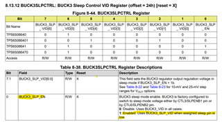
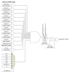
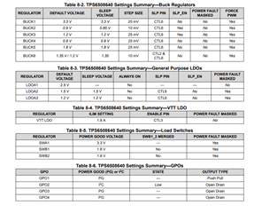
I am designing a power module using the TPS6508640 device. As is true for this family of regulators there are feedback pins that are typically connected to the output of the switching inductor. In another forum item it was asked about how to compensate for drop due to traces to the load. The answer there was that the output inductor should be placed close to the load. However, in my case this is not possible as the design is in a separate module far from the load.

The question is as follows:

Should the feedback be connected to the output of the inductor anyway or should output the feedback pin on the module so that it can be connected to the actual load on the main board?

Many thanks

Michael Stamler

  • Hi Michael,

    Using a long trace to a distant sense point can result in worse transient performance close to the PMIC from my understanding. You can compensate for this by adding extra local capacitance, but a cleaner solution might be to use a short FB trace to the local capacitors while setting the output voltages a littler higher than the default. This way, the load side sees the correct voltage.

    If you go with my suggestion, you can either reprogram the TPS650864x device at every power up, or you can use the user-programmable TPS650861 and go through the process to have your own defaults programmed into the part.

    Remote FB is definitely possible with this PMIC, but I can't account for the physical nuances of your system so it's difficult to say how drastic the transient performance impact would be or whether the FB trace would start picking up too much noise because of trace routing. Shorter FB traces largely eliminate these concerns by reducing impact of these variables.

    If you are in the prototyping phase, I would suggest adding both a long and short FB trace option. You can include a 0 Ohm resistor on both traces so that you can disconnect one trace or the other for testing and see which FB type you want to use.

    Regards,

    James

  • Hi James,

    Thanks for your detailed reply. We are in the design phase and have full control over layout. It seems to me that the purpose of the sense feedback is to provide exactly that function: to close the voltage loop at the load, even if the load is far away. Take, for example, commercial power modules. They also have sense feedback for exactly this purpose.

    It is true that the noise on the feedback line is critical. However, if it is kept sufficiently quiet for its entire journey back to the controller then it is preferable to put it at the load. 

    What do you think.

    BR

  • Hi Michael,

    I think load side sensing makes more sense as well for your case. If you don't have any devices connected to the output rail closer to the chip, a slightly larger local transient on the rail shouldn't present too much of an issue, especially if you add a bit of extra local capacitance.

    Unfortunately, the evaluation modules we have on hand don't have a way to test remote sensing, so I can't confirm the operation on my end empirically.

    Regards,

    James

  • I will implement both solutions: load-side and local sensing using 0-ohm resistors. The default will be load-side sensing.

  • Hi Michael,

    Sounds good, and if you run into any other issues with the PMIC just let us know here on E2E. We will be happy to walk through debug and provide support.

    Regards,

    James

  • Fortunately, I have a lot of experience with this PMIC family. We originally used the 100 device which we needed to program using 7V. This time I am using the 640 because of its fixed outputs negating the need for burning. Making slight changes at power up using I2C is nice. Probably will do this in the FSBL of the ZynqMP before DDR initialization.

    I am implementing this design as a separate module with the intention of making it into a purchasable product. I can keep you posted on this. Can we communicate by email on this issue when it becomes relevant. My email is:  michael.s@xicoreresearch.com or xicore.eu@gmail.com

    What is your email?

    BR

  • I already have a question:

    The spec refers to a 'Sleep Voltage' controlled by CTL6. What is this exactly?

  • Hi Michael,

    This just means that you can pull CTL6 HIGH or LOW to select between two different voltages on a power rail. One voltage is the normal default value and the other voltage is the "sleep voltage" which is usually some lower voltage value. Different version of the PMIC have slightly different voltage settings but that's the general behavior.

    Below is an example of the BUCK3 register setting for sleep mode enable. CTL3 can also be programmed as a sleep control pin.

    Regards,

    James

  • Hi James. I have decided to use the TPS6508640 device and I have some questions regarding the sequencing. Referring to the data sheet of document tps650864.pdf, section 8.3 'TPSs6508640 Design and Settings', figure 8-4 'Power Up Sequence'. I follow the first half of the sequencing and then I get lost due to seemingly incomplete information as follows;

    1. The diagram shows that BUCK3 becomes asserted as a result of BUCK4-PG but it is not clear how this is achieved electrically (connections).
    2. The diagram shows that BUCK5 & SWB1 are enabled from BUCK3 but, again, it is not clear how this is achieved?
    3. BUCK5  enables LODA1 but it is not clear how?
    4. SWA1 is enabled from LDOA1 but it is not clear how?

    Can you provide the answers together with documentation showing this.

    BR

    Michael

  • Hi Michael,

    The TPS6508640 has internal PGOOD signals for all rails. The TPS6508640 is set up so that some rails respond to the power good of another power rail. This allows for further sequencing control because you can set up certain rails to only power up once a previous rail is ready.

    This is important for LDOs if you are using a BUCK as the input source. You could set the LDO to ramp up when BUCKx reaches power good so that you never run into a situation where the LDO powers up without proper input  available.

    These are digital settings that are changed in the programming registers (address 0x38). These programming registers are only listed in the TPS650861 datasheet since this is the user-programmable version.

    For the TPS6508640, the register map in the datasheet will only show the normal 0x5E address registers.

    Take a look at the TPS650861 datasheet register map section to see what I mean: https://www.ti.com/lit/gpn/tps650861

    The TPS6508640 is a pre-programmed version so the sequencing and power good delays are already decided.

    Below is an image that might help visualize the PGOOD sequencing logic. This comes from our OTP generator document that is usually used when programming the TPS650861 version.

    Regards,

    James

  • OK. That's cool. The issue is what to do with the CTLx inputs and GPOx outputs. Despite what you say, that the sequencing is fixed, there is still a need to connect up these signal on the board, which is not clear to me. It seems that some are fixed and some are not. Please clarify.

    BR

  • Hi Michael,

    The datasheet should show which CTLx pins correspond to which output rails in the sequence. You will need to pull the CTLx pins shown in the power sequence HIGH to activate the rails. Unused CTLx pins can be shorted to GND.

    For example, in Figure 8-4 of the datasheet, it is shown that CTL3 and CTL4 are the main two inputs needed to move through the power sequence (also CTL1 if necessary). In Figure 8-3 there is an example block diagram that shows how the CTL pins are connected so that CTL3 is the main sequence pin and CTL4 is automatically pulled HIGH by VCCINT_PG later in the sequence.

    CTL1 is a DDR_EN pin that controls BUCK6 directly. CTL1 could be connected to one of the output rails depending on where in the sequence you want the DDR to enable. Or you could use your host device to enable DDR at some other time. Most designs I see just pull all the CTLx pins HIGH at the start of the power sequence by connecting the pull-up resistors to the LDO3P3 output and let the programmed PGOOD logic handle the sequencing / timing.

    GPO outputs are either Open Drain or Push-Pull. If the GPOx in question is Open Drain then you will need a pull-up resistor to a 1.8V or 3.3V source in order to use the GPOx output. GPOx pins that are in "I2C" mode must be enabled using an I2C command. If the GPO is marked as "PG" then the GPO pin is programmed to respond to the state of one of the power rails (should be shown in the power sequence diagram). Below are some tables that show the TPS6508640 default settings:

    I recommend the TPS65086x Schematic and Layout Checklist (Rev. A) if you want to know how specific pins should be handled. The only thing to note is that "unused" is from the perspective of the PMIC, not the user. Even if you don't plan to use a pin, if the PMIC is trying to use it then you need to provide the proper passive components so that no faults occur.

    Regards,

    James

  • Hi James

    In table 8-2 CTL6 and CTL2 are in the SLP column. Does this mean enable or sleep or what?

    It is stated that if CTLx pins are not to be used they should be tied to VCC and then this will let the internally programmed PGOOD logic to kick in. Where are these sequencing documented and how specifically can the CTLx override this default behavior? 

    Table 8-4 shows the default power sequence. How is this affected by the CTL pins? If the CTL pins are not used then what is the exact, programmed default sequence?

    In the checklist the following is documented. Is this correct for the 8640 part?

    1. CTL1 controls Buck1/2/6
    2. CTL5 controls SWA1, SWB1, SWB2
    3. CTL4 controls LDOA2 and LDOA3
    4. CTL2 controls Buck3/4/6
    5. CTL6 controls VTT LDO
    6. CTL3 is the main enable. Chip is shutdown until asserted.

  • Hi Michael,

    The SLP pins can be programmed and tied to a specific BUCK. When a SLP CTLx pin is pulled HIGH the default BUCK voltage is used at the output (determined by BUCKx_VID register bit field). When the SLP pin is pulled LOW the BUCK output changes to a secondary output voltage (often set to be lower than the default voltage using the BUCKx_SLP_VID register bit field).

    CTLx pins that are not used can be tied to GND. The CTLx pins are used to start the power sequence since the first power rail will not enable until the main power CTLx pin is pulled HIGH. For the TPS6508640, CTL3 should be the pin that starts the sequence. If you pull all the necessary CTLx pin HIGH at the start of the sequence, then the power sequence only needs to worry about the PGOOD logic to determine the order and timing of the rails. If the CTLx pins are not used, the PMIC will not power up.

    The sequencing is documented in the power sequence diagram for each TPS65086x version (Figure 8-4 for the TPS6508640). If there is a specific part of the power sequence that doesn't make sense I can go into more detail.

    Regards,

    James

  • Hi Michael,

    To answer your question about the power sequence...

    1) CTL1 only controls BUCK6 and LDOA1

    2) CTL5 needs to be HIGH as part of the GPO2 PGOOD requirements (along with CTL3 and CTL4). GPO2 internal PGOOD signal needs to be HIGH in order to allow VTT LDO to enable. GPO2 is programmed for I2C enable which means GPO2 won't activate its output until you enabled it through I2C. However, the internal PGOOD signal for GPO2 is independent of the I2C setting so the PGOOD of GPO2 is still used by the PMIC as part of the VTT LDO enable requirements.

    3) LDOA2 and LDOA3 are not tied to a CTLx pin in the TPS6508640 version. These two rails are disabled by default and must be enabled by I2C.

    4) CTL2 should be a SLP pin for BUCK6, along with CTL6. CTL2 does not influence BUCK3 or BUCK4. BUCK6 has an additional "fixed voltage" feature that activates when CTL2 and CTL6 are pulled LOW. BUCK2 also has a SLP mode voltage but only requires CTL6 to be pulled low to active SLP mode. 

    5) CTL6 acts as a SLP pin as well. VTT LDO is tied to CTL3 and GPO2. Both need to be HIGH for VTT LDO to activate. GPO2 is tied to BUCK6 PGOOD so once BUCK6 ramps up, GPO2 

    6) You are correct that CTL3 is the main enable pin.

    This information is also documented in our TPS65086100 OTP Generator for Xilinx Zynq Ultrascale+ (TPS6508640 settings) excel sheet. This document is usually used to program a TPS65086100 (user programmable) version of the IC with the default TPS6508640 settings.

    On the "Sequencing" tab you can see the settings for each rail and the PGOOD dependencies. BUCK6 and LDOA1 have incorrect PGOOD settings shown in the document but this should be updated in the future. The datasheet is the correct sequence. Otherwise, everything should be accurate in that document.

    Regards,

    James