Tool/software:
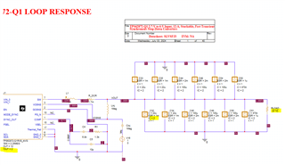
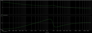
I'm currently simulating the AC loop response using the provided model. My schematic is configured with VIN = 5V, VOUT = 2V, and FSW = 2.5MHz. However, my plot shows the trace of DB(V(VOUT)) with the y-axis ranging from -220 to -340, and the trace of P(V(VOUT)) with the y-axis ranging from -20d to -180d, both in the negative.
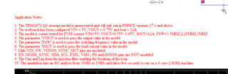
The application notes (attached below) show that the model is tested for VOUT = 0.75-1.05V and FSW = 1.5, 2.25, and 3MHz. Does this mean I can't adjust this model to my test configurations?