This thread has been locked.

If you have a related question, please click the "Ask a related question" button in the top right corner. The newly created question will be automatically linked to this question.

UCC21710QDWEVM-054: Two desat circuits

Part Number: UCC21710QDWEVM-054
Other Parts Discussed in Thread: UCC21750

Tool/software:

Hi

This EVM user guide provides two desat circuits and only one is implemented in the EVM.
I see its due to the IC being used. But if we are to use UCC21750, then the other desat circuit can be populated. 

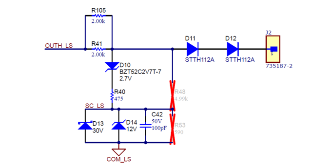
Following image shows the desired desat circuit i would like to know more about. 
In here, current limiting resistor is only 475OHM. What is the reason for such a low resistance. Is it ok to use 475?
The extra charging path resistance is also only 1k. That will lead to  about 14-15mA constant current draw from the gate driver output pin. is this ok too?

Couldn't find any continuous current ratings for gate driver pins. What is the maximum allowable  continuous current for gate driver pins. 
Will the 15mA create significant power dissipation in the gate driver? 

Regards
Damith

  • Hi Damith,

    1. We have specific EVM variant for UCC21750 - it will have configuration as needed for 0x750 device

    2. yes you can increase the current limiting resistor, as we have zener diode in the path which limits the voltage across DESAT pin and the HV, reduced current limiting resistor is fine. But you can increase to 1K if your application need.

    3. Extra charge current only applied during Out is high, not continuously. As the gate driver has ~10A of peak current ~15mA of current pulling from it should not be a concern. It wont increase gate driver power dissipation, but reduce the gate charge current.

    However if you don't need faster DESAT charging current, you can completely remove the R41 and R105 resistor and use only the DESAT charging current or add higher resistance to reduce the extra charge current path. Hope it answers your questions.

    Thanks

    Sasi

  • Hi Sasikala

    Thanks for the answers. I have few concerns here. 

    Please note that I'm not using the series Zener, to increase the trip level. 

    By continuous, i meant that it will flow longer than the turn on current of the pin. 10A will only flow for couple of nano seconds while this 15mA will flow as long as the gate pin is high (few micro seconds). it depends on the duty cycle. So if the duty cycle is higher, power dissipation is also will higher. That's what concerning me . 

    I'm trying to achieve 600nS blanking time. I will definitely need the speed up circuit. 
    But, parasitic capacitance from that Zener and the Schottky is getting in my way. The required capacitance is in the range of 50p-70p or so.
    But the parasitic of those diodes alone have more than half of it. I have seen that Zener has the largest capacitance among them. 

    Is it ok to add another Schottky from desat pin to positive rail, to protect it from over voltages, instead of the Zener. 
    So we have more control over the blanking capacitance. 


    Regards
    Damith

  • Hi Damith,

    Yes, the current consumption will be around ~15mA - will be based on the resistance in the path and will be high during "PWM on" time. But to achieve faster DESAT blanking time, that is the best approach. Or you could use UCC21755/756 variant, which has 5V threshold instead of 9V. The detection time will be reduced as the threshold is reduced as well.

    The zener is optional, you dont really need them as long as you maintain the needed isolation with HV diode and plan appropriate desat threshold based on your power module. It is generally recommended to plan 2 HV diodes, so that the blocking voltage will be half.

    With the EVM, we could successfully achieve around 600nsec even with Zener, but reduced the blanking capacitor to ~30pF.

    Hope it helps.

    Thanks

    Sasi

  • Hi Sasikala

    Thanks. These information helps a lot.  Thanks for the blanking time data too. 

    Do you have a comment about using a Schottky diode from desat pin to supply positive. So it wont go beyond supply voltage.

    Regards
    Damith

  • Damith, 

    it is a holiday in the US this week, so responses will be delayed. Our team will get back to you early next week.

    Regards,

    Daniel

  • Hi Damith, 

    Sasi is currently out of office so I'm helping out with the E2E questions. 

    The D14 Zener diode in the schematic you provided can serve the same purpose, and you can adjust the breakdown voltage according to your supply level. 

    Hope this helps! 

    Vivian

    • Hi Vivian

      Thank you for the response. But that Zener diode have considerable parasitic capacitance. Therefore it affects the blanking time significantly. We don't have control over the blanking time with that zener and Schottky in. We need less than 700nS (well, ideally it should be around 400)  of blanking time to protect SICs at 1200-1300V DC. 
      TI driver has inherent delay of about 300-400nS to respond for a short circuit. Therefore its only about 200-300nS left to play with. 
      That translates into less than100pF of capacitance. That zener and Schottky alone will going to have more than half of it. 


      Regards
      Damith
  • Hi Damith, 

    Understand. I would say with the extra charge current in this EVM you should be able to get the blanking time in the 200-300ns magnitude even with the Zener diode junction capacitance, but you can choose to use a Schottky diode to control the potential positive spike of DESAT voltage as well. It's no problem. 

    Thanks, 

    Vivian

  • Hi Vivian

    Thank you very much for the confirmation.
    Im curious. Is there any other gate driver with higher blanking capacitor charging currents, suitable for fast switching devices like SIC.
    Even though this gate driver is advertised for SIC, 500uA is too low for the blanking capacitor charging current compared to ~15mA provided by the external resistor. Is it because these gate drivers originally designed for IGBTs? 

    Regards
    Damith

  • Hi Damith, 

    The UCC217xx and ISO5x5x families both have blanking capacitor charging current of 500uA. Our programmable gate driver, UCC5880, has a programmable Ichg which can go up to 2mA. We are also actively looking at increasing the charging current for our upcoming devices. 

    Usually, we see customers needing 2-3us of protection time (from DESAT event to power switch shutdown), and it can easily be achieved by using a smaller blanking capacitor and/or implementing the external resistor charging path. 

    Thanks, 

    Vivian 

  • Hi Damith,

    Thanks Vivian for the detailed explanation to Damith during my absence. 

    As Vivian explained, currently all the non programmable isolated gate drivers have only 500uA Desat current. The OUTH external charge path can be used to reduce the blanking time to < 500-600 nsec.

    Do you see any concern with that external charge current approach?  Based on our understanding , ~500uA is typical for DESAT charge current for other competitor parts as well. Are you seeing a different trend? 

    Looking forward for your inputs.

  • Hi Sasikala and Vivian

    Thank you very much for the explanation. I can understand your reasons. 
    2 3 us blanking time is certainly ok for IGBTs. But with SICs, its not suitable when you go above or near 1kV. IGBTs have excellent short circuit withstand capability compared to the SIC. So timing is really critical.
    You can find more details from This PDF by TI.  
    More than 1uS blanking time isn't suitable when you go to voltages above 1kV (This is highly depend on the bus bar parasitic, but a "good" bus bar will produce very high fault currents in a short circuit event.)  .
    Our inhouse tests also confirmed this fact.  

    External path is fine. Its just its bit unusual and nice to have it all in the IC, so the external components will be low. 

    Thanks again for the information. 

    Regards
    Damith

  • Thanks Damith for the inputs, Got your point. Let me keep the information posted to our system team. 

    At present the best option is external charge path by adding resistor to OUTH

    Thanks

    Sasi