This thread has been locked.

If you have a related question, please click the "Ask a related question" button in the top right corner. The newly created question will be automatically linked to this question.

TPS63070: EMI Concerns

Part Number: TPS63070

Tool/software:

Dear TI,

We are writing to you today to seek your assistance with an issue we are encountering with our PSU design based on the TPS63070 chip.
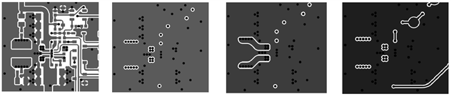
Design Overview

Our PSU design utilizes the TPS63070 chip to convert an input voltage from a battery source (ranging from 4V to 6V) to a stable output voltage of 4.8V (load of approximately 3.5W).

EMI Concerns

We have observed that the PSU generates significantly higher levels of radiated emissions when operating in boost mode. To mitigate this EMI issue, we have attempted the following measures:

Adding Snubbers: While not an ideal solution for our battery-powered application, we tried adding snubbers to the design. This resulted in some improvement in radiated emissions in boost mode but had minimal impact near the buck/boost transition point.

4-Layer PCB: We also transitioned to a 4-layer PCB to improve layout and signal integrity. This again led to some EMI reduction in boost mode but did not address the issue near the buck/boost transition point.

Additionally, we noticed a slight increase in radiated emissions across all input voltages when an electrolytic capacitor (3300uF) was added to the input.

EMI Evaluation

We evaluate the relative level of radiated emissions a using the RSSI value of an ISM band transceiver placed nearby in shielded box.

Request for Assistance

Given the persistent EMI challenges, especially near the buck/boost transition point, we kindly request your assistance in identifying and implementing effective EMI mitigation strategies.

We value your expertise and look forward to your prompt response and guidance in resolving this EMI issue.

Thank you for your time and consideration.

Sincerely,
Maksym

  • Hi  Maksym,

    Thanks for reaching out, could you share your schematic and top layer with silkscreen here?  Better you can share a screenshot with input connecter, it can help me to understand the path of noise coupling better.

    For now, i am confused about the location of input and output cap. this is important for EMI issue addressing.

    In you action--add snubber, which switching node you add?  L1 or L2 or both of them?

    Regards

    Tao

  • Hi Tao,

    Schematic

    3D View

    We experimented with various snubber configurations, and the best results were obtained with a 2.2nF capacitor and 2R resistor connected to switching node L2. However, we still observe a significant increase in noise at the Buck/Boost boundary (Vin≈Vout).

    Sincerely,
    Maksym

  • Hi  Maksym, 

    If my suspicion is correct, the EMI issue is at high frequency, may be around 100Mhz, right? Orelse, please let me know the frequency which is over standard in your test.

    Better you can summary tests you did before into a slides.

    Regards

    Tao

  • Dear Tao,

    Thank you for your prompt response. 

    The problem is indeed present at Sub-GHz frequencies. As mentioned earlier, we've observed a degradation in RSSI performance on our transceiver. To further illustrate this, we've attached the test results comparing the performance without a snubber and with the snubber connected across L2.

    Sincerely,
    Maksym

  • Hi  Maksym,

    Could you try to do test again based on following set-up?

    • Remove all 1500uF caps.
    • replace 1uF which is most close to device with a 10uF cap, may be you can find a 10uF cap in same package.

    Better to have tests step by step, and see what happen in each step.

    Actually, layout is not good enough, because some current of power stage has to go through vias which will cause some spikes and also a big loop of power stage. But for now, i think we can do nothing for this.

    Regards

    Tao

  • Hi Tao,

    Here are the test results you requested (without snubbers). The situation improves somewhat without the 1500uF capacitors.


    We followed the layout recommendations in slyp680.

    We are willing to modify our design if you provide appropriate recommendations, as obtaining good RSSI values is important to us.

    Sincerely,
    Maksym

  • Hi  Maksym,

    Thanks for your tests, since both steps does not help too much. we have to go back to basic theory of EMI, to find noise source and conduction path for noise.

    Noise source part, since it is a HF noise, i think it should be one or all of followings.

    • High di/dt noise during switching from one phase to another. In boost mode, two phases only, BOE(boost energized) and BOD(boost de-energized). In buck-boost mode, four phases exist, BOE and BDE, also BUE (buck energized) and BUD(buck de-energized). This part can be optimized by RC snubber or a inductor with higher inductance(to reduce the peak current of inductor). Also, a good layout should help too, smaller area of power loop, better EMI perfornance we got.
    • High du/dt during switching, similar with di/dt. it can be optimized by RC snubber and another inductor. Also, good layout should help too, difference with di/dt here is good layout can help to reduce the parasitic inductor and also to optimize the coupling path for du/dt signal.
    • Some HF oscillations. Here should be many kind of oscillation, such as rings during phase transition or end of each PFM switching phase. What is your actual load in test? is it possible device working in PFM mode?

    Noise coupling path part.

    • For High di/at part. it should be a space coupling. Mostly we are not able to cut off this coupling path without a  shield. what we can do is just to weak the noise source, smaller area and lower peak current as mentioned before.
    • For high du/dt part, it should be a PCB coupling pluse space coupling. Because when high du/dt signal goes through a trace, there will be some high frequency electromagnetic field around. 
    • For  HF oscillations, it should be similar with high du/dt signal, because high du/dt are just consist by different frequency of  sine waves.

    Back to this case.

    Only things we can do based on curren layout should be below.

    • Try with a different RC snubber, i mean with a smaller resister, such as 1Ohm, or 0Ohm if Tj is acceptable(no OTP triggered). 
    • Try another inductor with higher inductance. But make sure no loop stability issue will happen.

    For re-design of layout. I think we have to try to do this if we can not fix issues based on current layout. then i think it is better if we can have Webex meeting to discuss.

    Regards

    Tao

  • Hi Tao,

    Conducted repeated tests on a 4-layer board at different input voltages:
    Step 1: Initial BOM
    Step 2: C31=2.2nF, R24=2R
    Step 3: C31=2.2nF, R24=1R
    Step 4: C31=2.2nF, R24=1R, L=2.2uH

    As I mentioned earlier, a snubber of this size is not ideal for us, as it reduces efficiency by 5%.
    Note: In a previous message a few days ago, I accidentally sent you test results with a snubber on a 2-layer board.

    Sincerely,
    Maksym

  • Hi  Maksym,

    The results is really out of my expect. Joy

    Since we will have a Webex meeting tomorrow, let us have a detailed discussion then.

    Regards

    Tao

  • Hi Maksym,

    Would like to close this thread first, we can open it again if you have further questions.

    Regards

    Tao

  • Hi Tao,

    We have no more questions left. 
    Thank you very much for the support. 
    Sincerely,
    Maksym
  • Hi  Maksym,

    Thanks, I sent a friendship request. Hope you can accept it if no concern.

    Regards

    Tao